Freelance Electronics Components Distributor
Closed Dec 25th-26th
800-300-1968
We Stock Hard to Find Parts

ATMEGA48-20AU

Part # ATMEGA48-20AU
Description MCU 8BIT ATMEGA RISC 4KB FLASH 3.3V/5V 32TQFP - Trays
Category IC
Availability Out of Stock
Qty 0
Qty Price
1 + $1.49230


Technical Document


DISCLAIMER: The information provided herein is solely for informational purposes. Customers must be aware of the suitability of this product for their application, and consider that variable factors such as Manufacturer, Product Category, Date Codes, Pictures and Descriptions may differ from available inventory.

187
2545M–AVR–09/07
ATmega48/88/168
Figure 19-5. Start Bit Sampling
When the clock recovery logic detects a high (idle) to low (start) transition on the RxDn line, the
start bit detection sequence is initiated. Let sample 1 denote the first zero-sample as shown in
the figure. The clock recovery logic then uses samples 8, 9, and 10 for Normal mode, and sam-
ples 4, 5, and 6 for Double Speed mode (indicated with sample numbers inside boxes on the
figure), to decide if a valid start bit is received. If two or more of these three samples have logical
high levels (the majority wins), the start bit is rejected as a noise spike and the Receiver starts
looking for the next high to low-transition. If however, a valid start bit is detected, the clock recov-
ery logic is synchronized and the data recovery can begin. The synchronization process is
repeated for each start bit.
19.8.2 Asynchronous Data Recovery
When the receiver clock is synchronized to the start bit, the data recovery can begin. The data
recovery unit uses a state machine that has 16 states for each bit in Normal mode and eight
states for each bit in Double Speed mode. Figure 19-6 shows the sampling of the data bits and
the parity bit. Each of the samples is given a number that is equal to the state of the recovery
unit.
Figure 19-6. Sampling of Data and Parity Bit
The decision of the logic level of the received bit is taken by doing a majority voting of the logic
value to the three samples in the center of the received bit. The center samples are emphasized
on the figure by having the sample number inside boxes. The majority voting process is done as
follows: If two or all three samples have high levels, the received bit is registered to be a logic 1.
If two or all three samples have low levels, the received bit is registered to be a logic 0. This
majority voting process acts as a low pass filter for the incoming signal on the RxDn pin. The
recovery process is then repeated until a complete frame is received. Including the first stop bit.
Note that the Receiver only uses the first stop bit of a frame.
Figure 19-7 shows the sampling of the stop bit and the earliest possible beginning of the start bit
of the next frame.
12345678 9 10 11 12 13 14 15 16 12
STARTIDLE
00
BIT 0
3
1234 5 678120
RxD
Sample
(U2X = 0)
Sample
(U2X = 1)
12345678 9 10 11 12 13 14 15 16 1
BIT n
1234 5 6781
RxD
Sample
(U2X = 0)
Sample
(U2X = 1)
188
2545M–AVR–09/07
ATmega48/88/168
Figure 19-7. Stop Bit Sampling and Next Start Bit Sampling
The same majority voting is done to the stop bit as done for the other bits in the frame. If the stop
bit is registered to have a logic 0 value, the Frame Error (FEn) Flag will be set.
A new high to low transition indicating the start bit of a new frame can come right after the last of
the bits used for majority voting. For Normal Speed mode, the first low level sample can be at
point marked (A) in Figure 19-7. For Double Speed mode the first low level must be delayed to
(B). (C) marks a stop bit of full length. The early start bit detection influences the operational
range of the Receiver.
19.8.3 Asynchronous Operational Range
The operational range of the Receiver is dependent on the mismatch between the received bit
rate and the internally generated baud rate. If the Transmitter is sending frames at too fast or too
slow bit rates, or the internally generated baud rate of the Receiver does not have a similar (see
Table 19-2) base frequency, the Receiver will not be able to synchronize the frames to the start
bit.
The following equations can be used to calculate the ratio of the incoming data rate and internal
receiver baud rate.
D Sum of character size and parity size (D = 5 to 10 bit)
S Samples per bit. S = 16 for Normal Speed mode and S = 8 for Double Speed
mode.
S
F
First sample number used for majority voting. S
F
= 8 for normal speed and S
F
= 4
for Double Speed mode.
S
M
Middle sample number used for majority voting. S
M
= 9 for normal speed and
S
M
= 5 for Double Speed mode.
R
slow
is the ratio of the slowest incoming data rate that can be accepted in relation to the
receiver baud rate. R
fast
is the ratio of the fastest incoming data rate that can be
accepted in relation to the receiver baud rate.
Table 19-2 and Table 19-3 list the maximum receiver baud rate error that can be tolerated. Note
that Normal Speed mode has higher toleration of baud rate variations.
12345678 9 10 0/1 0/1 0/1
STOP 1
1234 5 6 0/1
RxD
Sample
(U2X = 0)
Sample
(U2X = 1)
(A) (B) (C)
R
slow
D
1
+()S
S 1 DS S
F
++
---------------------------------------
--- -
= R
fast
D
2
+()S
D 1+()SS
M
+
--------------------------------
---
=
189
2545M–AVR–09/07
ATmega48/88/168
The recommendations of the maximum receiver baud rate error was made under the assump-
tion that the Receiver and Transmitter equally divides the maximum total error.
There are two possible sources for the receivers baud rate error. The Receiver’s system clock
(XTAL) will always have some minor instability over the supply voltage range and the tempera-
ture range. When using a crystal to generate the system clock, this is rarely a problem, but for a
resonator the system clock may differ more than 2% depending of the resonators tolerance. The
second source for the error is more controllable. The baud rate generator can not always do an
exact division of the system frequency to get the baud rate wanted. In this case an UBRRn value
that gives an acceptable low error can be used if possible.
19.9 Multi-processor Communication Mode
Setting the Multi-processor Communication mode (MPCMn) bit in UCSRnA enables a filtering
function of incoming frames received by the USART Receiver. Frames that do not contain
address information will be ignored and not put into the receive buffer. This effectively reduces
the number of incoming frames that has to be handled by the CPU, in a system with multiple
MCUs that communicate via the same serial bus. The Transmitter is unaffected by the MPCMn
setting, but has to be used differently when it is a part of a system utilizing the Multi-processor
Communication mode.
If the Receiver is set up to receive frames that contain 5 to 8 data bits, then the first stop bit indi-
cates if the frame contains data or address information. If the Receiver is set up for frames with
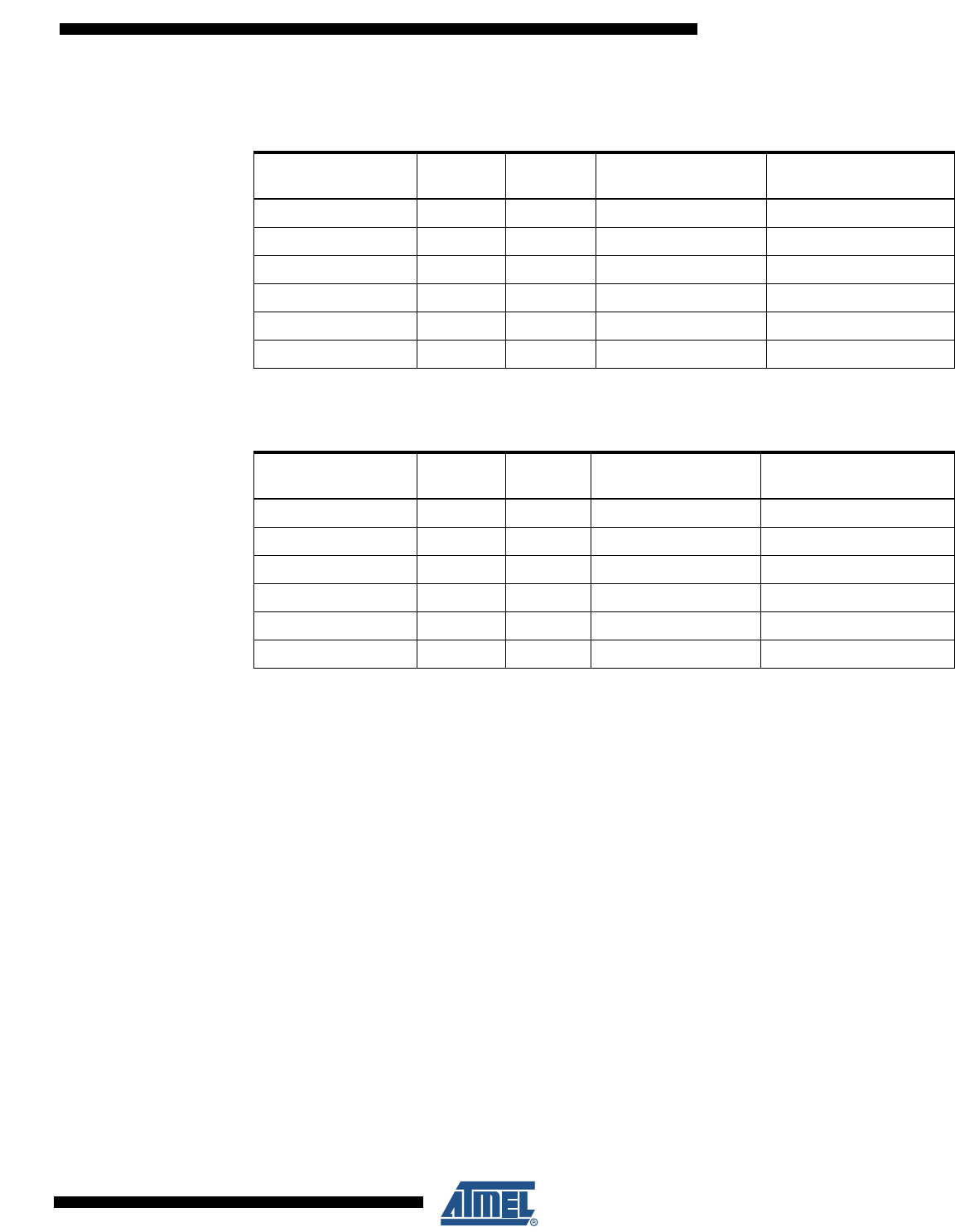
Table 19-2. Recommended Maximum Receiver Baud Rate Error for Normal Speed Mode
(U2Xn = 0)
D
# (Data+Parity Bit) R
slow
(%) R
fast
(%) Max Total Error (%)
Recommended Max
Receiver Error (%)
5 93.20 106.67 +6.67/-6.8 ± 3.0
6 94.12 105.79 +5.79/-5.88 ± 2.5
7 94.81 105.11 +5.11/-5.19 ± 2.0
8 95.36 104.58 +4.58/-4.54 ± 2.0
9 95.81 104.14 +4.14/-4.19 ± 1.5
10 96.17 103.78 +3.78/-3.83 ± 1.5
Table 19-3. Recommended Maximum Receiver Baud Rate Error for Double Speed Mode
(U2Xn = 1)
D
# (Data+Parity Bit) R
slow
(%) R
fast
(%) Max Total Error (%)
Recommended Max
Receiver Error (%)
5 94.12 105.66 +5.66/-5.88 ± 2.5
6 94.92 104.92 +4.92/-5.08 ± 2.0
7 95.52 104,35 +4.35/-4.48 ± 1.5
8 96.00 103.90 +3.90/-4.00 ± 1.5
9 96.39 103.53 +3.53/-3.61 ± 1.5
10 96.70 103.23 +3.23/-3.30 ± 1.0
PREVIOUS5657585960616263646566676869NEXT