Freelance Electronics Components Distributor
Closed Dec 25th-26th
800-300-1968
We Stock Hard to Find Parts

ATMEGA48-20AU

Part # ATMEGA48-20AU
Description MCU 8BIT ATMEGA RISC 4KB FLASH 3.3V/5V 32TQFP - Trays
Category IC
Availability Out of Stock
Qty 0
Qty Price
1 + $1.49230


Technical Document


DISCLAIMER: The information provided herein is solely for informational purposes. Customers must be aware of the suitability of this product for their application, and consider that variable factors such as Manufacturer, Product Category, Date Codes, Pictures and Descriptions may differ from available inventory.

175
2545M–AVR–09/07
ATmega48/88/168
Table 19-1 contains equations for calculating the baud rate (in bits per second) and for calculat-
ing the UBRRn value for each mode of operation using an internally generated clock source.
Note: 1. The baud rate is defined to be the transfer rate in bit per second (bps)
BAUD Baud rate (in bits per second, bps)
f
OSC
System Oscillator clock frequency
UBRRn Contents of the UBRRnH and UBRRnL Registers, (0-4095)
Some examples of UBRRn values for some system clock frequencies are found in Table 19-9
(see page 196).
19.3.2 Double Speed Operation (U2Xn)
The transfer rate can be doubled by setting the U2Xn bit in UCSRnA. Setting this bit only has
effect for the asynchronous operation. Set this bit to zero when using synchronous operation.
Setting this bit will reduce the divisor of the baud rate divider from 16 to 8, effectively doubling
the transfer rate for asynchronous communication. Note however that the Receiver will in this
case only use half the number of samples (reduced from 16 to 8) for data sampling and clock
recovery, and therefore a more accurate baud rate setting and system clock are required when
this mode is used. For the Transmitter, there are no downsides.
Table 19-1. Equations for Calculating Baud Rate Register Setting
Operating Mode
Equation for Calculating Baud
Rate
(1)
Equation for Calculating
UBRRn Value
Asynchronous Normal mode
(U2Xn = 0)
Asynchronous Double Speed
mode (U2Xn = 1)
Synchronous Master mode
BAUD
f
OSC
16 UBRRn 1+()
------------------------------------------=
UBRRn
f
OSC
16BAUD
----------------------- -
1
=
BAUD
f
OSC
8 UBRRn 1+()
-------------------------------------- -=
UBRRn
f
OSC
8BAUD
--------------------
1
=
BAUD
f
OSC
2 UBRRn 1+()
-------------------------------------- -=
UBRRn
f
OSC
2BAUD
--------------------
1
=
176
2545M–AVR–09/07
ATmega48/88/168
19.3.3 External Clock
External clocking is used by the synchronous slave modes of operation. The description in this
section refers to Figure 19-2 for details.
External clock input from the XCKn pin is sampled by a synchronization register to minimize the
chance of meta-stability. The output from the synchronization register must then pass through
an edge detector before it can be used by the Transmitter and Receiver. This process intro-
duces a two CPU clock period delay and therefore the maximum external XCKn clock frequency
is limited by the following equation:
Note that f
osc
depends on the stability of the system clock source. It is therefore recommended to
add some margin to avoid possible loss of data due to frequency variations.
19.3.4 Synchronous Clock Operation
When synchronous mode is used (UMSELn = 1), the XCKn pin will be used as either clock input
(Slave) or clock output (Master). The dependency between the clock edges and data sampling
or data change is the same. The basic principle is that data input (on RxDn) is sampled at the
opposite XCKn clock edge of the edge the data output (TxDn) is changed.
Figure 19-3. Synchronous Mode XCKn Timing.
The UCPOLn bit UCRSC selects which XCKn clock edge is used for data sampling and which is
used for data change. As Figure 19-3 shows, when UCPOLn is zero the data will be changed at
rising XCKn edge and sampled at falling XCKn edge. If UCPOLn is set, the data will be changed
at falling XCKn edge and sampled at rising XCKn edge.
19.4 Frame Formats
A serial frame is defined to be one character of data bits with synchronization bits (start and stop
bits), and optionally a parity bit for error checking. The USART accepts all 30 combinations of
the following as valid frame formats:
1 start bit
5, 6, 7, 8, or 9 data bits
no, even or odd parity bit
1 or 2 stop bits
f
XCK
f
OSC
4
--------
---
<
RxD / TxD
XCK
RxD / TxD
XCK
UCPOL = 0
UCPOL = 1
Sample
Sample
177
2545M–AVR–09/07
ATmega48/88/168
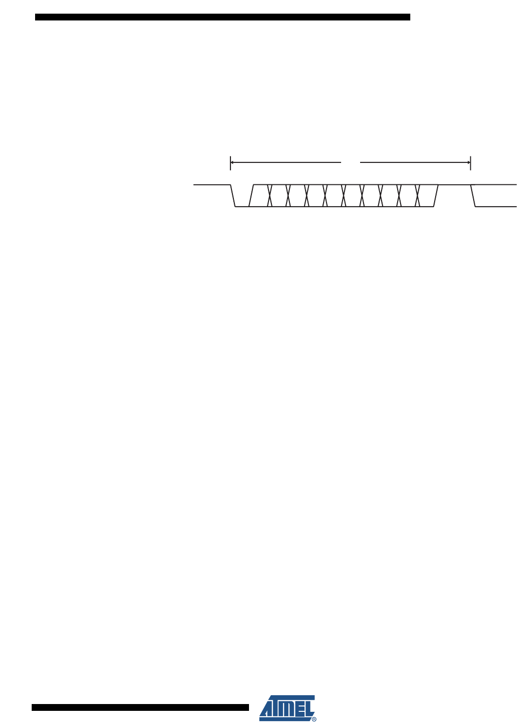
A frame starts with the start bit followed by the least significant data bit. Then the next data bits,
up to a total of nine, are succeeding, ending with the most significant bit. If enabled, the parity bit
is inserted after the data bits, before the stop bits. When a complete frame is transmitted, it can
be directly followed by a new frame, or the communication line can be set to an idle (high) state.
Figure 19-4 illustrates the possible combinations of the frame formats. Bits inside brackets are
optional.
Figure 19-4. Frame Formats
St Start bit, always low.
(n) Data bits (0 to 8).
P Parity bit. Can be odd or even.
Sp Stop bit, always high.
IDLE No transfers on the communication line (RxDn or TxDn). An IDLE line
must be
high.
The frame format used by the USART is set by the UCSZn2:0, UPMn1:0 and USBSn bits in
UCSRnB and UCSRnC. The Receiver and Transmitter use the same setting. Note that changing
the setting of any of these bits will corrupt all ongoing communication for both the Receiver and
Transmitter.
The USART Character SiZe (UCSZn2:0) bits select the number of data bits in the frame. The
USART Parity mode (UPMn1:0) bits enable and set the type of parity bit. The selection between
one or two stop bits is done by the USART Stop Bit Select (USBSn) bit. The Receiver ignores
the second stop bit. An FE (Frame Error) will therefore only be detected in the cases where the
first stop bit is zero.
19.4.1 Parity Bit Calculation
The parity bit is calculated by doing an exclusive-or of all the data bits. If odd parity is used, the
result of the exclusive or is inverted. The relation between the parity bit and data bits is as
follows:
P
even
Parity bit using even parity
P
odd
Parity bit using odd parity
d
n
Data bit n of the character
If used, the parity bit is located between the last data bit and first stop bit of a serial frame.
10 2 3 4 [5] [6] [7] [8] [P]St Sp1 [Sp2] (St / IDLE)(IDLE)
FRAME
P
even
d
n 1
d
3
d
2
d
1
d
0
0
P
odd
⊕⊕⊕⊕⊕⊕
d
n 1
d
3
d
2
d
1
d
0
1⊕⊕⊕⊕⊕⊕
=
=
PREVIOUS5253545556575859606162636465NEXT