Freelance Electronics Components Distributor
Closed Dec 25th-26th
800-300-1968
We Stock Hard to Find Parts

ATMEGA48-20AU

Part # ATMEGA48-20AU
Description MCU 8BIT ATMEGA RISC 4KB FLASH 3.3V/5V 32TQFP - Trays
Category IC
Availability Out of Stock
Qty 0
Qty Price
1 + $1.49230


Technical Document


DISCLAIMER: The information provided herein is solely for informational purposes. Customers must be aware of the suitability of this product for their application, and consider that variable factors such as Manufacturer, Product Category, Date Codes, Pictures and Descriptions may differ from available inventory.

160
2545M–AVR–09/07
ATmega48/88/168
Bit 1 – OCF2A: Output Compare Flag 2 A
The OCF2A bit is set (one) when a compare match occurs between the Timer/Counter2 and the
data in OCR2A – Output Compare Register2. OCF2A is cleared by hardware when executing
the corresponding interrupt handling vector. Alternatively, OCF2A is cleared by writing a logic
one to the flag. When the I-bit in SREG, OCIE2A (Timer/Counter2 Compare match Interrupt
Enable), and OCF2A are set (one), the Timer/Counter2 Compare match Interrupt is executed.
Bit 0 – TOV2: Timer/Counter2 Overflow Flag
The TOV2 bit is set (one) when an overflow occurs in Timer/Counter2. TOV2 is cleared by hard-
ware when executing the corresponding interrupt handling vector. Alternatively, TOV2 is cleared
by writing a logic one to the flag. When the SREG I-bit, TOIE2A (Timer/Counter2 Overflow Inter-
rupt Enable), and TOV2 are set (one), the Timer/Counter2 Overflow interrupt is executed. In
PWM mode, this bit is set when Timer/Counter2 changes counting direction at 0x00.
17.11.8 ASSR – Asynchronous Status Register
Bit 7 – RES: Reserved bit
This bit is reserved and will always read as zero.
Bit 6 – EXCLK: Enable External Clock Input
When EXCLK is written to one, and asynchronous clock is selected, the external clock input
buffer is enabled and an external clock can be input on Timer Oscillator 1 (TOSC1) pin instead
of a 32 kHz crystal. Writing to EXCLK should be done before asynchronous operation is
selected. Note that the crystal Oscillator will only run when this bit is zero.
Bit 5 – AS2: Asynchronous Timer/Counter2
When AS2 is written to zero, Timer/Counter2 is clocked from the I/O clock, clk
I/O
. When AS2 is
written to one, Timer/Counter2 is clocked from a crystal Oscillator connected to the Timer Oscil-
lator 1 (TOSC1) pin. When the value of AS2 is changed, the contents of TCNT2, OCR2A,
OCR2B, TCCR2A and TCCR2B might be corrupted.
Bit 4 – TCN2UB: Timer/Counter2 Update Busy
When Timer/Counter2 operates asynchronously and TCNT2 is written, this bit becomes set.
When TCNT2 has been updated from the temporary storage register, this bit is cleared by hard-
ware. A logical zero in this bit indicates that TCNT2 is ready to be updated with a new value.
Bit 3 – OCR2AUB: Output Compare Register2 Update Busy
When Timer/Counter2 operates asynchronously and OCR2A is written, this bit becomes set.
When OCR2A has been updated from the temporary storage register, this bit is cleared by hard-
ware. A logical zero in this bit indicates that OCR2A is ready to be updated with a new value.
Bit 2 – OCR2BUB: Output Compare Register2 Update Busy
When Timer/Counter2 operates asynchronously and OCR2B is written, this bit becomes set.
When OCR2B has been updated from the temporary storage register, this bit is cleared by hard-
ware. A logical zero in this bit indicates that OCR2B is ready to be updated with a new value.
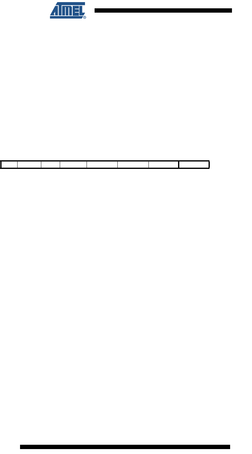
Bit 7 6 5 4 3 2 1 0
(0xB6) EXCLK AS2 TCN2UB OCR2AUB OCR2BUB TCR2AUB TCR2BUB ASSR
Read/Write R R/W R/W R R R R R
Initial Value 0 0 0 0 0 0 0 0
161
2545M–AVR–09/07
ATmega48/88/168
Bit 1 – TCR2AUB: Timer/Counter Control Register2 Update Busy
When Timer/Counter2 operates asynchronously and TCCR2A is written, this bit becomes set.
When TCCR2A has been updated from the temporary storage register, this bit is cleared by
hardware. A logical zero in this bit indicates that TCCR2A is ready to be updated with a new
value.
Bit 0 – TCR2BUB: Timer/Counter Control Register2 Update Busy
When Timer/Counter2 operates asynchronously and TCCR2B is written, this bit becomes set.
When TCCR2B has been updated from the temporary storage register, this bit is cleared by
hardware. A logical zero in this bit indicates that TCCR2B is ready to be updated with a new
value.
If a write is performed to any of the five Timer/Counter2 Registers while its update busy flag is
set, the updated value might get corrupted and cause an unintentional interrupt to occur.
The mechanisms for reading TCNT2, OCR2A, OCR2B, TCCR2A and TCCR2B are different.
When reading TCNT2, the actual timer value is read. When reading OCR2A, OCR2B, TCCR2A
and TCCR2B the value in the temporary storage register is read.
17.11.9 GTCCR – General Timer/Counter Control Register
Bit 1 – PSRASY: Prescaler Reset Timer/Counter2
When this bit is one, the Timer/Counter2 prescaler will be reset. This bit is normally cleared
immediately by hardware. If the bit is written when Timer/Counter2 is operating in asynchronous
mode, the bit will remain one until the prescaler has been reset. The bit will not be cleared by
hardware if the TSM bit is set. Refer to the description of the “Bit 7 – TSM: Timer/Counter Syn-
chronization Mode” on page 140 for a description of the Timer/Counter Synchronization mode.
Bit 7 6 5 4 3 2 1 0
0x23 (0x43) TSM
PSRASY PSRSYNC GTCCR
Read/Write R/W R R R R R R/W R/W
Initial Value 0 0 0 0 0 0 0 0
162
2545M–AVR–09/07
ATmega48/88/168
18. SPI – Serial Peripheral Interface
18.1 Features
Full-duplex, Three-wire Synchronous Data Transfer
Master or Slave Operation
LSB First or MSB First Data Transfer
Seven Programmable Bit Rates
End of Transmission Interrupt Flag
Write Collision Flag Protection
Wake-up from Idle Mode
Double Speed (CK/2) Master SPI Mode
18.2 Overview
The Serial Peripheral Interface (SPI) allows high-speed synchronous data transfer between the
ATmega48/88/168 and peripheral devices or between several AVR devices.
The USART can also be used in Master SPI mode, see “USART in SPI Mode” on page 200. The
PRSPI bit in “Minimizing Power Consumption” on page 42 must be written to zero to enable SPI
module.
PREVIOUS4748495051525354555657585960NEXT