Freelance Electronics Components Distributor
Closed Dec 25th-26th
800-300-1968
We Stock Hard to Find Parts

ATMEGA48-20AU

Part # ATMEGA48-20AU
Description MCU 8BIT ATMEGA RISC 4KB FLASH 3.3V/5V 32TQFP - Trays
Category IC
Availability Out of Stock
Qty 0
Qty Price
1 + $1.49230


Technical Document


DISCLAIMER: The information provided herein is solely for informational purposes. Customers must be aware of the suitability of this product for their application, and consider that variable factors such as Manufacturer, Product Category, Date Codes, Pictures and Descriptions may differ from available inventory.

106
2545M–AVR–09/07
ATmega48/88/168
If external pin modes are used for the Timer/Counter0, transitions on the T0 pin will clock the
counter even if the pin is configured as an output. This feature allows software control of the
counting.
14.9.3 TCNT0 – Timer/Counter Register
The Timer/Counter Register gives direct access, both for read and write operations, to the
Timer/Counter unit 8-bit counter. Writing to the TCNT0 Register blocks (removes) the Compare
Match on the following timer clock. Modifying the counter (TCNT0) while the counter is running,
introduces a risk of missing a Compare Match between TCNT0 and the OCR0x Registers.
14.9.4 OCR0A – Output Compare Register A
The Output Compare Register A contains an 8-bit value that is continuously compared with the
counter value (TCNT0). A match can be used to generate an Output Compare interrupt, or to
generate a waveform output on the OC0A pin.
14.9.5 OCR0B – Output Compare Register B
The Output Compare Register B contains an 8-bit value that is continuously compared with the
counter value (TCNT0). A match can be used to generate an Output Compare interrupt, or to
generate a waveform output on the OC0B pin.
Table 14-9. Clock Select Bit Description
CS02 CS01 CS00 Description
0 0 0 No clock source (Timer/Counter stopped)
001clk
I/O
/(No prescaling)
010clk
I/O
/8 (From prescaler)
011clk
I/O
/64 (From prescaler)
100clk
I/O
/256 (From prescaler)
101clk
I/O
/1024 (From prescaler)
1 1 0 External clock source on T0 pin. Clock on falling edge.
1 1 1 External clock source on T0 pin. Clock on rising edge.
Bit 76543210
0x26 (0x46) TCNT0[7:0] TCNT0
Read/Write R/W R/W R/W R/W R/W R/W R/W R/W
Initial Value 0 0 0 0 0 0 0 0
Bit 76543210
0x27 (0x47) OCR0A[7:0] OCR0A
Read/Write R/W R/W R/W R/W R/W R/W R/W R/W
Initial Value 0 0 0 0 0 0 0 0
Bit 76543210
0x28 (0x48) OCR0B[7:0] OCR0B
Read/Write R/W R/W R/W R/W R/W R/W R/W R/W
Initial Value 0 0 0 0 0 0 0 0
107
2545M–AVR–09/07
ATmega48/88/168
14.9.6 TIMSK0 – Timer/Counter Interrupt Mask Register
Bits 7..3 – Res: Reserved Bits
These bits are reserved bits in the ATmega48/88/168 and will always read as zero.
Bit 2 – OCIE0B: Timer/Counter Output Compare Match B Interrupt Enable
When the OCIE0B bit is written to one, and the I-bit in the Status Register is set, the
Timer/Counter Compare Match B interrupt is enabled. The corresponding interrupt is executed if
a Compare Match in Timer/Counter occurs, i.e., when the OCF0B bit is set in the Timer/Counter
Interrupt Flag Register – TIFR0.
Bit 1 – OCIE0A: Timer/Counter0 Output Compare Match A Interrupt Enable
When the OCIE0A bit is written to one, and the I-bit in the Status Register is set, the
Timer/Counter0 Compare Match A interrupt is enabled. The corresponding interrupt is executed
if a Compare Match in Timer/Counter0 occurs, i.e., when the OCF0A bit is set in the
Timer/Counter 0 Interrupt Flag Register – TIFR0.
Bit 0 – TOIE0: Timer/Counter0 Overflow Interrupt Enable
When the TOIE0 bit is written to one, and the I-bit in the Status Register is set, the
Timer/Counter0 Overflow interrupt is enabled. The corresponding interrupt is executed if an
overflow in Timer/Counter0 occurs, i.e., when the TOV0 bit is set in the Timer/Counter 0 Inter-
rupt Flag Register – TIFR0.
14.9.7 TIFR0 – Timer/Counter 0 Interrupt Flag Register
Bits 7..3 – Res: Reserved Bits
These bits are reserved bits in the ATmega48/88/168 and will always read as zero.
Bit 2 – OCF0B: Timer/Counter 0 Output Compare B Match Flag
The OCF0B bit is set when a Compare Match occurs between the Timer/Counter and the data in
OCR0B – Output Compare Register0 B. OCF0B is cleared by hardware when executing the cor-
responding interrupt handling vector. Alternatively, OCF0B is cleared by writing a logic one to
the flag. When the I-bit in SREG, OCIE0B (Timer/Counter Compare B Match Interrupt Enable),
and OCF0B are set, the Timer/Counter Compare Match Interrupt is executed.
Bit 1 – OCF0A: Timer/Counter 0 Output Compare A Match Flag
The OCF0A bit is set when a Compare Match occurs between the Timer/Counter0 and the data
in OCR0A – Output Compare Register0. OCF0A is cleared by hardware when executing the cor-
responding interrupt handling vector. Alternatively, OCF0A is cleared by writing a logic one to
the flag. When the I-bit in SREG, OCIE0A (Timer/Counter0 Compare Match Interrupt Enable),
and OCF0A are set, the Timer/Counter0 Compare Match Interrupt is executed.
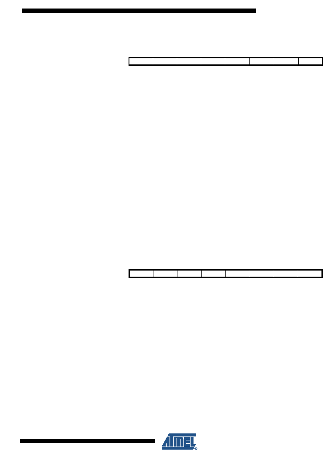
Bit 7 6 5 4 3 2 1 0
(0x6E) OCIE0B OCIE0A TOIE0 TIMSK0
Read/Write RRRRRR/WR/WR/W
Initial Value 0 0 0 0 0 0 0 0
Bit 76543210
0x15 (0x35) OCF0B OCF0A TOV0 TIFR0
Read/Write R R R R R R/W R/W R/W
Initial Value 0 0 0 0 0 0 0 0
108
2545M–AVR–09/07
ATmega48/88/168
Bit 0 – TOV0: Timer/Counter0 Overflow Flag
The bit TOV0 is set when an overflow occurs in Timer/Counter0. TOV0 is cleared by hardware
when executing the corresponding interrupt handling vector. Alternatively, TOV0 is cleared by
writing a logic one to the flag. When the SREG I-bit, TOIE0 (Timer/Counter0 Overflow Interrupt
Enable), and TOV0 are set, the Timer/Counter0 Overflow interrupt is executed.
The setting of this flag is dependent of the WGM02:0 bit setting. Refer to Table 14-8, “Waveform
Generation Mode Bit Description” on page 104.
PREVIOUS2930313233343536373839404142NEXT