Freelance Electronics Components Distributor
Closed Dec 25th-26th
800-300-1968
We Stock Hard to Find Parts

ATMEGA48-20AU

Part # ATMEGA48-20AU
Description MCU 8BIT ATMEGA RISC 4KB FLASH 3.3V/5V 32TQFP - Trays
Category IC
Availability Out of Stock
Qty 0
Qty Price
1 + $1.49230


Technical Document


DISCLAIMER: The information provided herein is solely for informational purposes. Customers must be aware of the suitability of this product for their application, and consider that variable factors such as Manufacturer, Product Category, Date Codes, Pictures and Descriptions may differ from available inventory.

313
2545M–AVR–09/07
ATmega48/88/168
28.9 Parallel Programming Characteristics
Figure 28-7. Parallel Programming Timing, Including some General Timing Requirements
Figure 28-8. Parallel Programming Timing, Loading Sequence with Timing Requirements
(1)
Note: 1. The timing requirements shown in Figure 28-7 (i.e., t
DVXH
, t
XHXL
, and t
XLDX
) also apply to load-
ing operation.
Data & Contol
(
DATA, XA0/1, BS1, BS2)
XTAL1
t
XHXL
t
WLWH
t
DVXH
t
XLDX
t
PLWL
t
WLRH
WR
RDY/BSY
PAGEL
t
PHPL
t
PLBX
t
BVPH
t
XLWL
t
WLBX
t
BVWL
WLRL
XTAL1
P
AGEL
t
PLXH
XLXH
t
t
XLPH
ADDR0 (Low Byte) DATA (Low Byte) DATA (High Byte) ADDR1 (Low Byte)
DATA
BS1
XA0
XA1
LOAD ADDRESS
(LOW BYTE)
LOAD DATA
(LOW BYTE)
LOAD DATA
(HIGH BYTE)
LOAD DATA
LOAD ADDRESS
(LOW BYTE)
314
2545M–AVR–09/07
ATmega48/88/168
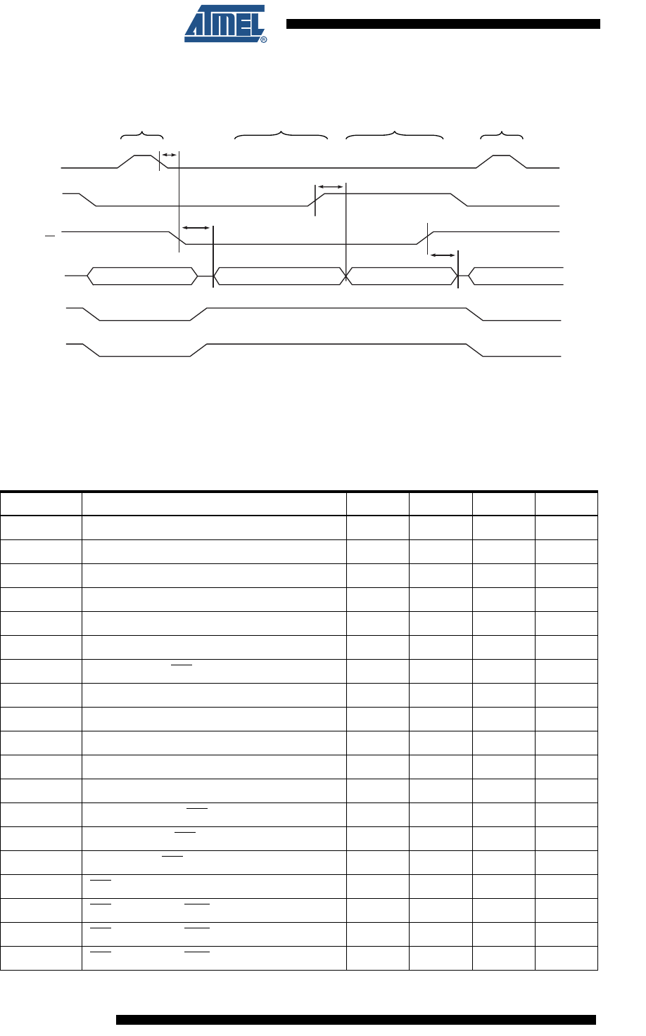
Figure 28-9. Parallel Programming Timing, Reading Sequence (within the Same Page) with
Timing Requirements
(1)
Note: 1. The timing requirements shown in Figure 28-7 (i.e., t
DVXH
, t
XHXL
, and t
XLDX
) also apply to read-
ing operation.
Table 28-8. Parallel Programming Characteristics, V
CC
= 5V ± 10%
Symbol Parameter Min Typ Max Units
V
PP
Programming Enable Voltage 11.5 12.5 V
I
PP
Programming Enable Current 250 μA
t
DVXH
Data and Control Valid before XTAL1 High 67 ns
t
XLXH
XTAL1 Low to XTAL1 High 200 ns
t
XHXL
XTAL1 Pulse Width High 150 ns
t
XLDX
Data and Control Hold after XTAL1 Low 67 ns
t
XLWL
XTAL1 Low to WR Low 0 ns
t
XLPH
XTAL1 Low to PAGEL high 0 ns
t
PLXH
PAGEL low to XTAL1 high 150 ns
t
BVPH
BS1 Valid before PAGEL High 67 ns
t
PHPL
PAGEL Pulse Width High 150 ns
t
PLBX
BS1 Hold after PAGEL Low 67 ns
t
WLBX
BS2/1 Hold after WR Low 67 ns
t
PLWL
PAGEL Low to WR Low 67 ns
t
BVWL
BS1 Valid to WR Low 67 ns
t
WLWH
WR Pulse Width Low 150 ns
t
WLRL
WR Low to RDY/BSY Low 0 1 μs
t
WLRH
WR Low to RDY/BSY High
(1)
3.7 4.5 ms
t
WLRH_CE
WR Low to RDY/BSY High for Chip Erase
(2)
7.5 9 ms
X
TAL1
OE
ADDR0 (Low Byte) DATA (Low Byte)
DATA (High Byte)
ADDR1 (Low Byte)
DATA
BS1
XA0
XA1
LOAD ADDRESS
(LOW BYTE)
READ DATA
(LOW BYTE)
READ DATA
(HIGH BYTE)
LOAD ADDRESS
(LOW BYTE)
t
BVDV
t
OLDV
t
XLOL
t
OHDZ
315
2545M–AVR–09/07
ATmega48/88/168
Notes: 1. t
WLRH
is valid for the Write Flash, Write EEPROM, Write Fuse bits and Write Lock bits
commands.
2. t
WLRH_CE
is valid for the Chip Erase command.
t
XLOL
XTAL1 Low to OE Low 0 ns
t
BVDV
BS1 Valid to DATA valid 0 250 ns
t
OLDV
OE Low to DATA Valid 250 ns
t
OHDZ
OE High to DATA Tri-stated 250 ns
Table 28-8. Parallel Programming Characteristics, V
CC
= 5V ± 10% (Continued)
Symbol Parameter Min Typ Max Units
PREVIOUS9899100101102103104105106107108109110111NEXT