Freelance Electronics Components Distributor
Closed Dec 25th-26th
800-300-1968
We Stock Hard to Find Parts

ATMEGA48-20AU

Part # ATMEGA48-20AU
Description MCU 8BIT ATMEGA RISC 4KB FLASH 3.3V/5V 32TQFP - Trays
Category IC
Availability Out of Stock
Qty 0
Qty Price
1 + $1.49230


Technical Document


DISCLAIMER: The information provided herein is solely for informational purposes. Customers must be aware of the suitability of this product for their application, and consider that variable factors such as Manufacturer, Product Category, Date Codes, Pictures and Descriptions may differ from available inventory.

310
2545M–AVR–09/07
ATmega48/88/168
3. C
b
= capacitance of one bus line in pF.
4. f
CK
= CPU clock frequency
5. This requirement applies to all ATmega48/88/168 2-wire Serial Interface operation. Other devices connected to the 2-wire
Serial Bus need only obey the general f
SCL
requirement.
6. The actual low period generated by the ATmega48/88/168 2-wire Serial Interface is (1/f
SCL
- 2/f
CK
), thus f
CK
must be greater
than 6 MHz for the low time requirement to be strictly met at f
SCL
= 100 kHz.
7. The actual low period generated by the ATmega48/88/168 2-wire Serial Interface is (1/f
SCL
- 2/f
CK
), thus the low time require-
ment will not be strictly met for f
SCL
> 308 kHz when f
CK
= 8 MHz. Still, ATmega48/88/168 devices connected to the bus may
communicate at full speed (400 kHz) with other ATmega48/88/168 devices, as well as any other device with a proper t
LOW
acceptance margin.
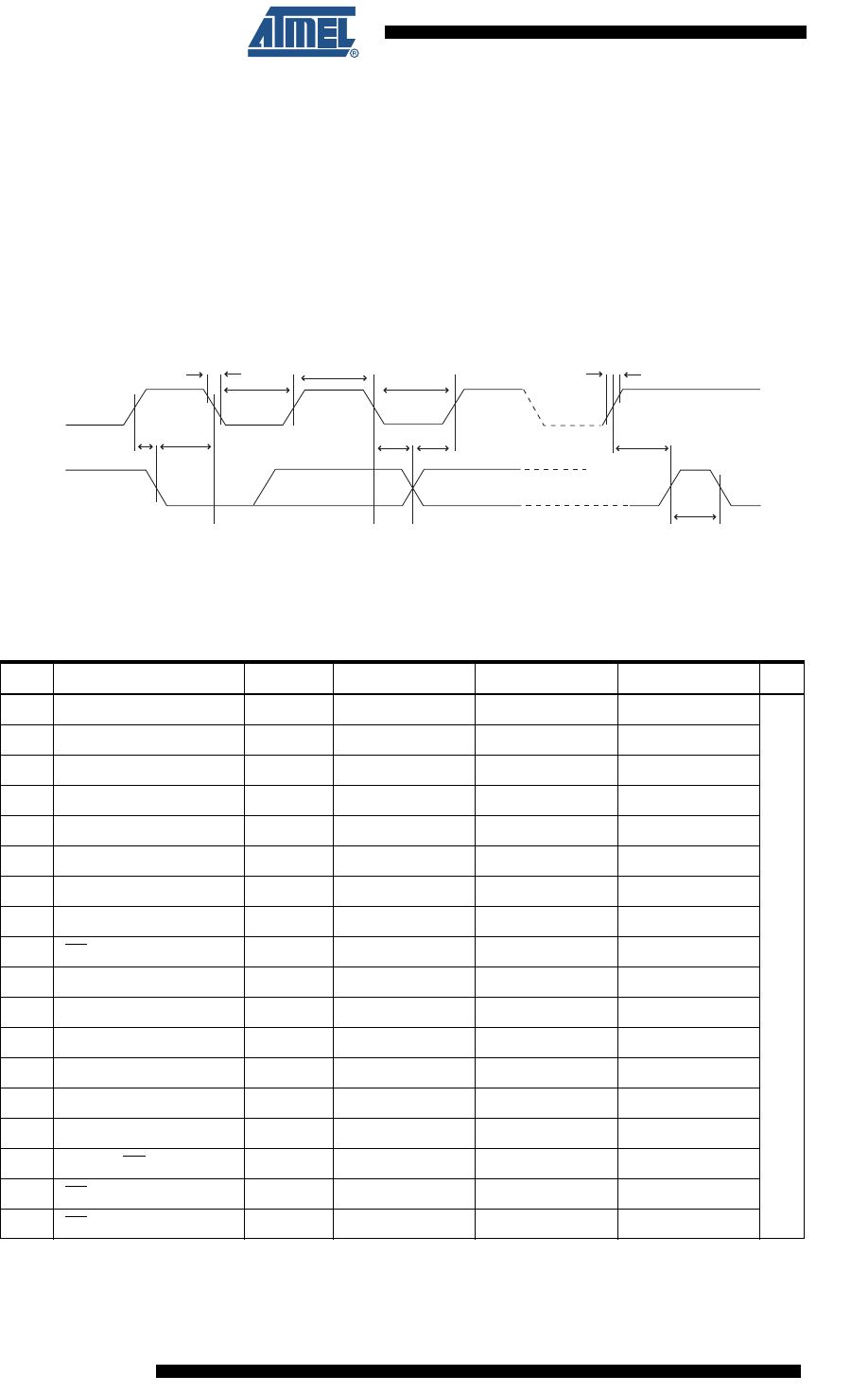
Figure 28-4. 2-wire Serial Bus Timing
28.7 SPI Timing Characteristics
See Figure 28-5 and Figure 28-6 for details.
Note: 1. In SPI Programming mode the minimum SCK high/low period is:
- 2 t
CLCL
for f
CK
< 12 MHz
- 3 t
CLCL
for f
CK
> 12 MHz
t
SU;STA
t
LOW
t
HIGH
t
LOW
t
of
t
HD;STA
t
HD;DAT
t
SU;DAT
t
SU;STO
t
BUF
SCL
SDA
t
r
Table 28-6. SPI Timing Parameters
Description Mode Min Typ Max
1 SCK period Master See Table 18-5
ns
2 SCK high/low Master 50% duty cycle
3 Rise/Fall time Master 3.6
4 Setup Master 10
5Hold Master 10
6 Out to SCK Master 0.5 • t
sck
7 SCK to out Master 10
8 SCK to out high Master 10
9SS
low to out Slave 15
10 SCK period Slave 4 • t
ck
11 SCK high/low
(1)
Slave 2 • t
ck
12 Rise/Fall time Slave 1600
13 Setup Slave 10
14 Hold Slave t
ck
15 SCK to out Slave 15
16 SCK to SS
high Slave 20
17 SS high to tri-state Slave 10
18 SS
low to SCK Slave 20
311
2545M–AVR–09/07
ATmega48/88/168
Figure 28-5. SPI Interface Timing Requirements (Master Mode)
Figure 28-6. SPI Interface Timing Requirements (Slave Mode)
MOSI
(
Data Output)
SCK
(CPOL = 1)
MISO
(Data Input)
SCK
(CPOL = 0)
SS
MSB LSB
LSBMSB
...
...
61
22
345
8
7
MISO
(
Data Output)
SCK
(CPOL = 1)
MOSI
(Data Input)
SCK
(CPOL = 0)
SS
MSB LSB
LSBMSB
...
...
10
11 11
1213 14
17
15
9
X
16
312
2545M–AVR–09/07
ATmega48/88/168
28.8 ADC Characteristics
Note: 1. AV
CC
absolute min/max: 1.8V/5.5V
Table 28-7. ADC Characteristics
Symbol Parameter Condition Min Typ Max Units
Resolution 10 Bits
Absolute accuracy (Including
INL, DNL, quantization error,
gain and offset error)
V
REF
= 4V, V
CC
= 4V,
ADC clock = 200 kHz
2LSB
V
REF
= 4V, V
CC
= 4V,
ADC clock = 1 MHz
4.5 LSB
V
REF
= 4V, V
CC
= 4V,
ADC clock = 200 kHz
Noise Reduction Mode
2LSB
V
REF
= 4V, V
CC
= 4V,
ADC clock = 1 MHz
Noise Reduction Mode
4.5 LSB
Integral Non-Linearity (INL)
V
REF
= 4V, V
CC
= 4V,
ADC clock = 200 kHz
0.5 LSB
Differential Non-Linearity
(DNL)
V
REF
= 4V, V
CC
= 4V,
ADC clock = 200 kHz
0.25 LSB
Gain Error
V
REF
= 4V, V
CC
= 4V,
ADC clock = 200 kHz
2LSB
Offset Error
V
REF
= 4V, V
CC
= 4V,
ADC clock = 200 kHz
2LSB
Conversion Time Free Running Conversion 13 260 µs
Clock Frequency 50 1000 kHz
AV
CC
(1)
Analog Supply Voltage V
CC
- 0.3 V
CC
+ 0.3 V
V
REF
Reference Voltage 1.0 AV
CC
V
V
IN
Input Voltage GND V
REF
V
Input Bandwidth 38.5 kHz
V
INT
Internal Voltage Reference 1.0 1.1 1.2 V
R
REF
Reference Input Resistance 32 kΩ
R
AIN
Analog Input Resistance 100 MΩ
PREVIOUS979899100101102103104105106107108109110NEXT