Freelance Electronics Components Distributor
Closed Dec 25th-26th
800-300-1968
We Stock Hard to Find Parts

ATMEGA48-20AU

Part # ATMEGA48-20AU
Description MCU 8BIT ATMEGA RISC 4KB FLASH 3.3V/5V 32TQFP - Trays
Category IC
Availability Out of Stock
Qty 0
Qty Price
1 + $1.49230


Technical Document


DISCLAIMER: The information provided herein is solely for informational purposes. Customers must be aware of the suitability of this product for their application, and consider that variable factors such as Manufacturer, Product Category, Date Codes, Pictures and Descriptions may differ from available inventory.

307
2545M–AVR–09/07
ATmega48/88/168
28.4 Clock Characteristics
28.4.1 Calibrated Internal RC Oscillator Accuracy
Notes: 1. Voltage range for ATmega48V/88V/168V.
2. Voltage range for ATmega48/88/168.
28.4.2 External Clock Drive Waveforms
Figure 28-3. External Clock Drive Waveforms
28.4.3 External Clock Drive
Table 28-1. Calibration Accuracy of Internal RC Oscillator
Frequency V
CC
Temperature Calibration Accuracy
Factory
Calibration
8.0 MHz 3V 25°10%
User
Calibration
7.3 - 8.1 MHz
1.8V - 5.5V
(1)
2.7V - 5.5V
(2)
-40°C - 85°1%
V
IL1
V
IH1
Table 28-2. External Clock Drive
Symbol Parameter
V
CC
=1.8-5.5V V
CC
=2.7-5.5V V
CC
=4.5-5.5V
UnitsMin. Max. Min. Max. Min. Max.
1/t
CLCL
Oscillator
Frequency
04010020MHz
t
CLCL
Clock Period 250 100 50 ns
t
CHCX
High Time 100 40 20 ns
t
CLCX
Low Time 100 40 20 ns
t
CLCH
Rise Time 2.0 1.6 0.5 μs
t
CHCL
Fall Time 2.0 1.6 0.5 μs
Δt
CLCL
Change in period
from one clock
cycle to the next
222%
308
2545M–AVR–09/07
ATmega48/88/168
28.5 System and Reset Characteristics
Note: 1. The Power-on Reset will not work unless the supply voltage has been below V
POT
(falling)
Notes: 1. V
BOT
may be below nominal minimum operating voltage for some devices. For devices where this is the case, the device is
tested down to V
CC
= V
BOT
during the production test. This guarantees that a Brown-Out Reset will occur before V
CC
drops to
a voltage where correct operation of the microcontroller is no longer guaranteed. The test is performed using
BODLEVEL = 110 and BODLEVEL = 101 for ATmega48V/88V/168V, and BODLEVEL = 101 and BODLEVEL = 100 for
ATmega48/88/168.
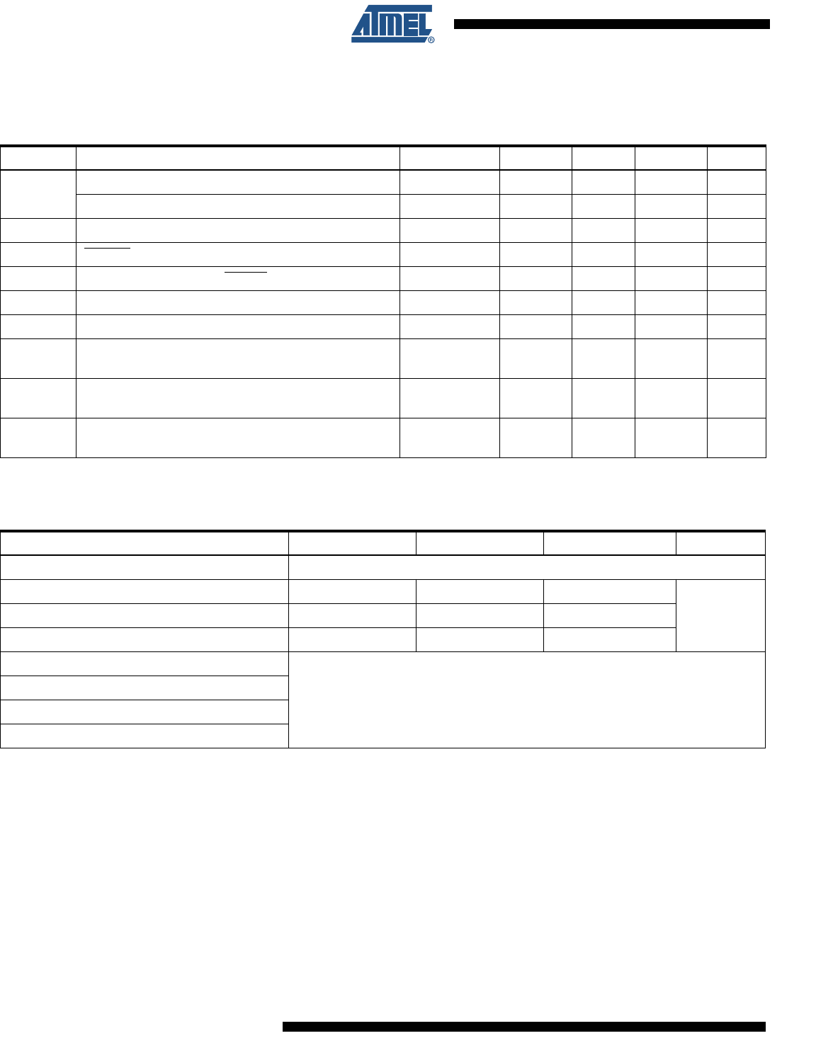
Table 28-3. Reset, Brown-out and Internal voltage Characteristics
Symbol Parameter Condition Min Typ Max Units
V
POT
Power-on Reset Threshold Voltage (rising) 0.7 1.0 1.4 V
Power-on Reset Threshold Voltage (falling)
(1)
0.05 0.9 1.3 V
V
PSR
Power-on Slope Rate 0.01 4.5 V/ms
V
RST
RESET Pin Threshold Voltage 0.2 V
CC
0.9 V
CC
V
t
RST
Minimum pulse width on RESET Pin 2.5 µs
V
HYST
Brown-out Detector Hysteresis 50 mV
t
BOD
Min Pulse Width on Brown-out Reset 2 µs
V
BG
Bandgap reference voltage
V
CC
=2.7
T
A
=25°C
1.0 1.1 1.2 V
t
BG
Bandgap reference start-up time
V
CC
=2.7
T
A
=25°C
40 70 µs
I
BG
Bandgap reference current consumption
V
CC
=2.7
T
A
=25°C
10 µA
Table 28-4. BODLEVEL Fuse Coding
(1)
BODLEVEL 2:0 Fuses Min V
BOT
Typ V
BOT
Max V
BOT
Units
111 BOD Disabled
110 1.7 1.8 2.0
V101 2.5 2.7 2.9
100 4.1 4.3 4.5
011
Reserved
010
001
000
309
2545M–AVR–09/07
ATmega48/88/168
28.6 2-wire Serial Interface Characteristics
Table 28-5 describes the requirements for devices connected to the 2-wire Serial Bus. The ATmega48/88/168 2-wire Serial
Interface meets or exceeds these requirements under the noted conditions.
Timing symbols refer to Figure 28-4.
Notes: 1. In ATmega48/88/168, this parameter is characterized and not 100% tested.
2. Required only for f
SCL
> 100 kHz.
Table 28-5. 2-wire Serial Bus Requirements
Symbol Parameter
Condition Min Max Units
VIL
Input Low-voltage -0.5 0.3 V
CC
V
VIH
Input High-voltage 0.7 V
CC
V
CC
+ 0.5 V
Vhys
(1)
Hysteresis of Schmitt Trigger Inputs 0.05 V
CC
(2)
–V
VOL
(1)
Output Low-voltage 3 mA sink current 0 0.4 V
tr
(1)
Rise Time for both SDA and SCL 20 + 0.1C
b
(3)(2)
300 ns
tof
(1)
Output Fall Time from V
IHmin
to V
ILmax
10 pF < C
b
< 400 pF
(3)
20 + 0.1C
b
(3)(2)
250 ns
tSP
(1)
Spikes Suppressed by Input Filter 0 50
(2)
ns
I
i
Input Current each I/O Pin 0.1V
CC
< V
i
< 0.9V
CC
-10 10 µA
C
i
(1)
Capacitance for each I/O Pin 10 pF
f
SCL
SCL Clock Frequency f
CK
(4)
> max(16f
SCL
, 250kHz)
(5)
0 400 kHz
Rp Value of Pull-up resistor
f
SCL
100 kHz
f
SCL
> 100 kHz
t
HD;STA
Hold Time (repeated) START Condition
f
SCL
100 kHz 4.0 µs
f
SCL
> 100 kHz 0.6 µs
t
LOW
Low Period of the SCL Clock
f
SCL
100 kHz
(6)
4.7 µs
f
SCL
> 100 kHz
(7)
1.3 µs
t
HIGH
High period of the SCL clock
f
SCL
100 kHz 4.0 µs
f
SCL
> 100 kHz 0.6 µs
t
SU;STA
Set-up time for a repeated START condition
f
SCL
100 kHz 4.7 µs
f
SCL
> 100 kHz 0.6 µs
t
HD;DAT
Data hold time
f
SCL
100 kHz 0 3.45 µs
f
SCL
> 100 kHz 0 0.9 µs
t
SU;DAT
Data setup time
f
SCL
100 kHz 250 ns
f
SCL
> 100 kHz 100 ns
t
SU;STO
Setup time for STOP condition
f
SCL
100 kHz 4.0 µs
f
SCL
> 100 kHz 0.6 µs
t
BUF
Bus free time between a STOP and START
condition
f
SCL
100 kHz 4.7 µs
f
SCL
> 100 kHz 1.3 µs
V
CC
0,4V
3mA
-
-----------------------
----
1000ns
C
b
-----------------
Ω
V
CC
0,4V
3mA
-
-----------------------
----
300ns
C
b
--------------
Ω
PREVIOUS96979899100101102103104105106107108109NEXT