Freelance Electronics Components Distributor
Closed Dec 25th-26th
800-300-1968
We Stock Hard to Find Parts

ATMEGA48-20AU

Part # ATMEGA48-20AU
Description MCU 8BIT ATMEGA RISC 4KB FLASH 3.3V/5V 32TQFP - Trays
Category IC
Availability Out of Stock
Qty 0
Qty Price
1 + $1.49230


Technical Document


DISCLAIMER: The information provided herein is solely for informational purposes. Customers must be aware of the suitability of this product for their application, and consider that variable factors such as Manufacturer, Product Category, Date Codes, Pictures and Descriptions may differ from available inventory.

304
2545M–AVR–09/07
ATmega48/88/168
28. Electrical Characteristics
28.1 Absolute Maximum Ratings*
28.2 DC Characteristics
Operating Temperature.................................. -55°C to +125°C
*NOTICE: Stresses beyond those listed under “Absolute
Maximum Ratings” may cause permanent dam-
age to the device. This is a stress rating only and
functional operation of the device at these or
other conditions beyond those indicated in the
operational sections of this specification is not
implied. Exposure to absolute maximum rating
conditions for extended periods may affect
device reliability.
Storage Temperature..................................... -65°C to +150°C
Voltage on any Pin except RESET
with respect to Ground ................................-0.5V to V
CC
+0.5V
Voltage on RESET
with respect to Ground......-0.5V to +13.0V
Maximum Operating Voltage ............................................ 6.0V
DC Current per I/O Pin ............................................... 40.0 mA
DC Current
V
CC
and GND Pins................................ 200.0 mA
T
A
= -40°C to 85°C, V
CC
= 1.8V to 5.5V (unless otherwise noted)
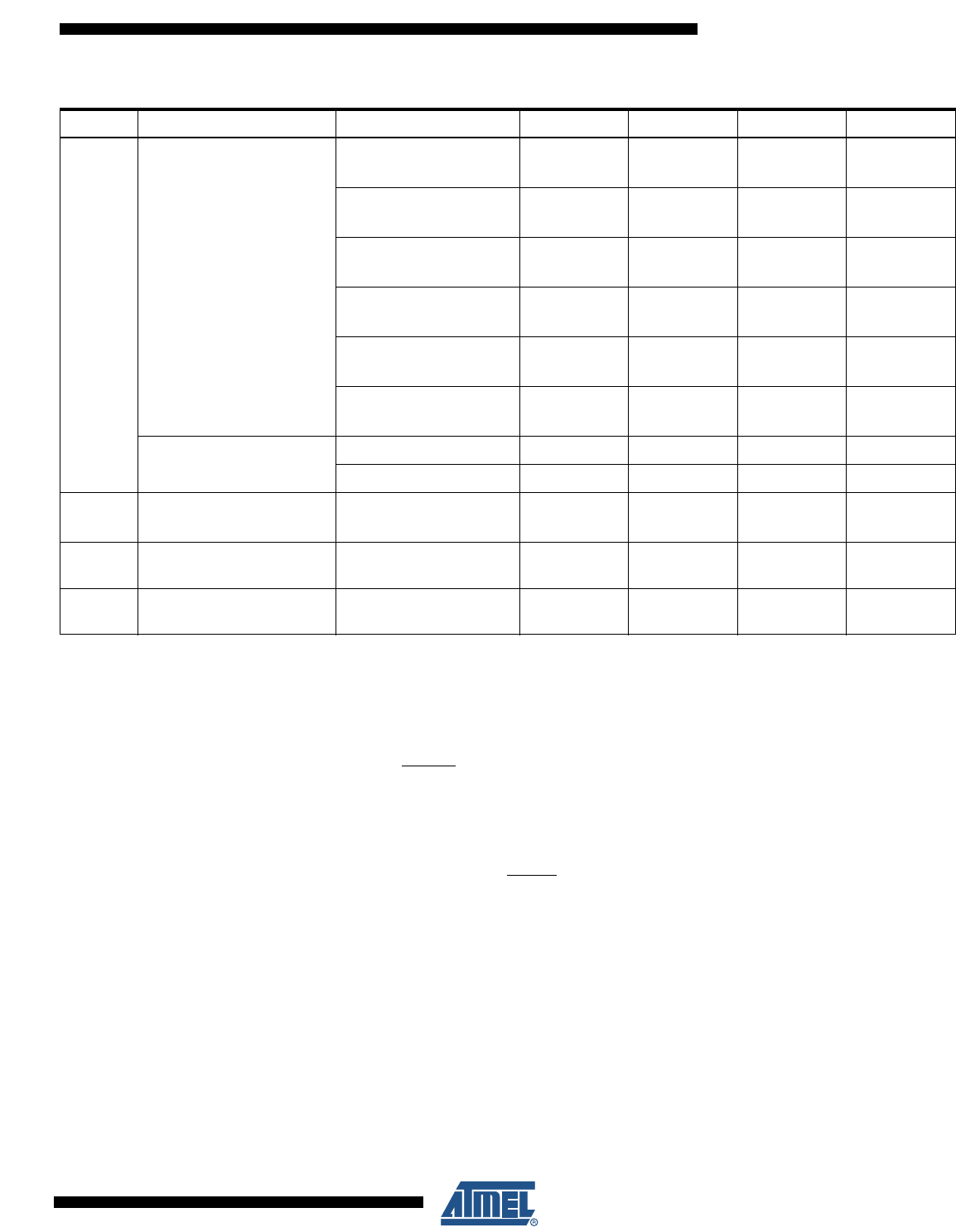
Symbol Parameter Condition Min. Typ. Max. Units
V
IL
Input Low Voltage, except
XTAL1 and RESET pin
V
CC
= 1.8V - 2.4V
V
CC
= 2.4V - 5.5V
-0.5
-0.5
0.2V
CC
(1)
0.3V
CC
(1)
V
V
IH
Input High Voltage, except
XTAL1 and RESET pins
V
CC
= 1.8V - 2.4V
V
CC
= 2.4V - 5.5V
0.7V
CC
(2)
0.6V
CC
(2)
V
CC
+ 0.5
V
CC
+ 0.5
V
V
IL1
Input Low Voltage,
XTAL1 pin
V
CC
= 1.8V - 5.5V -0.5 0.1V
CC
(1)
V
V
IH1
Input High Voltage,
XTAL1 pin
V
CC
= 1.8V - 2.4V
V
CC
= 2.4V - 5.5V
0.8V
CC
(2)
0.7V
CC
(2)
V
CC
+ 0.5
V
CC
+ 0.5
V
V
IL2
Input Low Voltage,
RESET pin
V
CC
= 1.8V - 5.5V -0.5 0.2V
CC
(1)
V
V
IH2
Input High Voltage,
RESET
pin
V
CC
= 1.8V - 5.5V 0.9V
CC
(2)
V
CC
+ 0.5 V
V
IL3
Input Low Voltage,
RESET pin as I/O
V
CC
= 1.8V - 2.4V
V
CC
= 2.4V - 5.5V
-0.5
-0.5
0.2V
CC
(1)
0.3V
CC
(1)
V
V
IH3
Input High Voltage,
RESET
pin as I/O
V
CC
= 1.8V - 2.4V
V
CC
= 2.4V - 5.5V
0.7V
CC
(2)
0.6V
CC
(2)
V
CC
+ 0.5
V
CC
+ 0.5
V
V
OL
Output Low Voltage
(3)
,
RESET
pin as I/O
I
OL
= 20mA, V
CC
= 5V
I
OL
= 6mA, V
CC
= 3V
0.7
0.5
V
V
OH
Output High Voltage
(4)
,
RESET
pin as I/O
I
OH
= -20mA, V
CC
= 5V
I
OH
= -10mA, V
CC
= 3V
4.2
2.3
V
I
IL
Input Leakage
Current I/O Pin
V
CC
= 5.5V, pin low
(absolute value)
A
I
IH
Input Leakage
Current I/O Pin
V
CC
= 5.5V, pin high
(absolute value)
A
R
RST
Reset Pull-up Resistor 30 60 kΩ
R
PU
I/O Pin Pull-up Resistor 20 50 kΩ
305
2545M–AVR–09/07
ATmega48/88/168
Notes: 1. “Max” means the highest value where the pin is guaranteed to be read as low
2. “Min” means the lowest value where the pin is guaranteed to be read as high
3. Although each I/O port can sink more than the test conditions (20 mA at V
CC
= 5V, 10 mA at V
CC
= 3V) under steady state
conditions (non-transient), the following must be observed:
ATmega48/88/168:
1] The sum of all I
OL
, for ports C0 - C5, ADC7, ADC6 should not exceed 100 mA.
2] The sum of all I
OL
, for ports B0 - B5, D5 - D7, XTAL1, XTAL2 should not exceed 100 mA.
3] The sum of all I
OL
, for ports D0 - D4, RESET should not exceed 100 mA.
If I
OL
exceeds the test condition, V
OL
may exceed the related specification. Pins are not guaranteed to sink current greater
than the listed test condition.
4. Although each I/O port can source more than the test conditions (20 mA at V
CC
= 5V, 10 mA at V
CC
= 3V) under steady state
conditions (non-transient), the following must be observed:
ATmega48/88/168:
1] The sum of all I
OH
, for ports C0 - C5, D0- D4, ADC7, RESET should not exceed 150 mA.
2] The sum of all I
OH
, for ports B0 - B5, D5 - D7, ADC6, XTAL1, XTAL2 should not exceed 150 mA.
If II
OH
exceeds the test condition, V
OH
may exceed the related specification. Pins are not guaranteed to source current
greater than the listed test condition.
5. Values with “Minimizing Power Consumption” enabled (0xFF).
I
CC
Power Supply Current
(5)
Active 1MHz, V
CC
= 2V
(ATmega48/88/168V)
0.55 mA
Active 4MHz, V
CC
= 3V
(ATmega48/88/168L)
3.5 mA
Active 8MHz, V
CC
= 5V
(ATmega48/88/168)
12 mA
Idle 1MHz, V
CC
= 2V
(ATmega48/88/168V)
0.25 0.5 mA
Idle 4MHz, V
CC
= 3V
(ATmega48/88/168L)
1.5 mA
Idle 8MHz, V
CC
= 5V
(ATmega48/88/168)
5.5 mA
Power-down mode
WDT enabled, V
CC
= 3V 8 15 µA
WDT disabled, V
CC
= 3V 1 2 µA
V
ACIO
Analog Comparator
Input Offset Voltage
V
CC
= 5V
V
in
= V
CC
/2
10 40 mV
I
ACLK
Analog Comparator
Input Leakage Current
V
CC
= 5V
V
in
= V
CC
/2
-50 50 nA
t
ACID
Analog Comparator
Propagation Delay
V
CC
= 2.7V
V
CC
= 4.0V
750
500
ns
T
A
= -40°C to 85°C, V
CC
= 1.8V to 5.5V (unless otherwise noted) (Continued)
Symbol Parameter Condition Min. Typ. Max. Units
306
2545M–AVR–09/07
ATmega48/88/168
28.3 Speed Grades
Maximum frequency is dependent on V
CC.
As shown in Figure 28-1 and Figure 28-2, the Maxi-
mum Frequency vs. V
CC
curve is linear between 1.8V < V
CC
< 2.7V and between 2.7V < V
CC
<
4.5V.
Figure 28-1. Maximum Frequency vs. V
CC
, ATmega48V/88V/168V
Figure 28-2. Maximum Frequency vs. V
CC
, ATmega48/88/168
10 MHz
4 MHz
1.8V 2.7V 5.5V
Safe Operating Area
20 MHz
10 MHz
2.7V 4.5V 5.5V
Safe Operating Area
PREVIOUS9596979899100101102103104105106107108NEXT