8
AT84AD001B
2153C–BDC–04/04
Note: The gain setting is 0 dB, one clock input, no standby mode [full power mode], 1:1 DMUX, calibration off.
Note: Gain setting is 0 dB, two clock inputs, no standby mode [full power mode], 1:2 DMUX, calibration on.
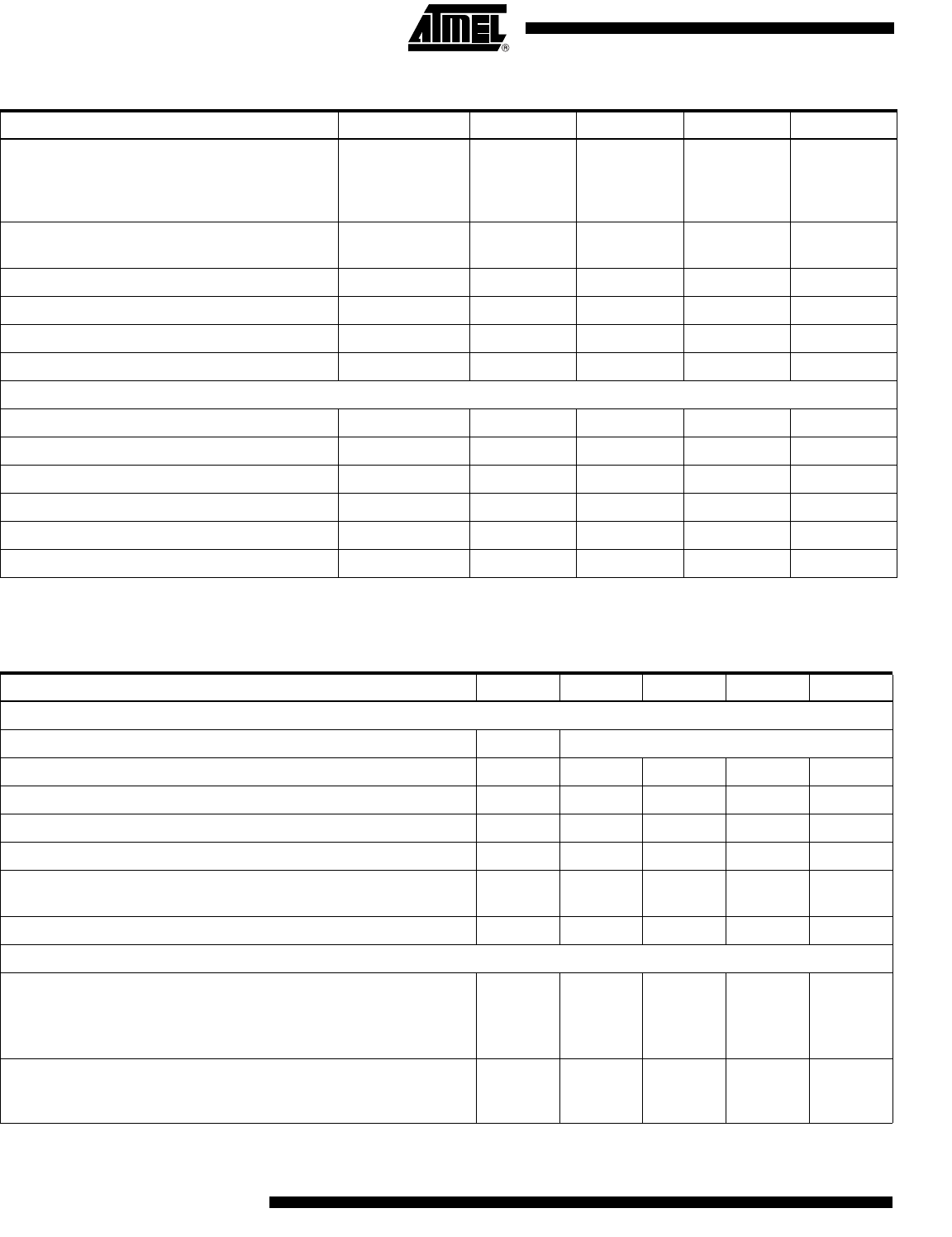
Output levels (assuming V
CCO
= 2.25V)
100Ω differentially terminated
Logic 0 voltage
Logic 1 voltage
V
OL
V
OH
1.0
1.25
1.1
1.35
1.2
1.45
V
V
Output offset voltage (assuming V
CCO
= 2.25V)
100Ω differentially terminated
V
OS
1125 1250 1325 mV
Output impedance R
O
50 W
Output current (shorted output) 12 mA
Output current (grounded output) 30 mA
Output level drift with temperature 1.3 mV/°C
Digital Input (Serial Interface)
Maximum clock frequency (input clk) Fclk 50 MHz
Input logical level 0 (clk, mode, data, ldn) -0.4 0 0.4 V
Input logical level 1 (clk, mode, data, ldn) V
CCO
- 0.4 V
CCO
- 0.4 V
CCO
+ 0.4 V
Output logical level 0 (cal) -0.4 0 0.4 V
Output logical level 1 (cal) V
CCO
- 0.4 V
CCO
V
CCO
+ 0.4 V
Maximum output load (cal) 15 pF
Table 3. Electrical Operating Characteristics in Nominal Conditions (Continued)
Parameter Symbol Min Typ Max Unit
Table 4. Electrical Operating Characteristics
Parameter Symbol Min Typ Max Unit
DC Accuracy
No missing code Guaranteed over specified temperature range
Differential non-linearity DNL 0.25 0.6 LSB
Integral non-linearity INL 0.5 1 LSB
Gain error (single channel I or Q) with calibration -0.5 0 0.5 LSB
Input offset matching (single channel I or Q) with calibration -0.5 0 0.5 LSB
Gain error drift against temperature
Gain error drift against V
CCA
0.062
0.064
LSB/°C
LSB/mV
Mean output offset code with calibration 127 127.5 128 LSB
Transient Performance
Bit Error Rate
Fs = 1 Gsps
Fin = 250 MHz
BER 10
-13
10
-10
Error/
sample
ADC settling time channel I or Q
(between 10% - 90% of output response)
V
Ini
-V
iniB
= 500 mVpp
TS 170 ps


