Freelance Electronics Components Distributor
Closed Dec 25th-26th
800-300-1968
We Stock Hard to Find Parts

AT84AD001BITD

Part # AT84AD001BITD
Description ADC DUAL FLASH 1GSPS 8BIT PARALLEL 144LQFP - Trays
Category IC
Availability Out of Stock
Qty 0
Qty Price
1 + $154.41500


Technical Document


DISCLAIMER: The information provided herein is solely for informational purposes. Customers must be aware of the suitability of this product for their application, and consider that variable factors such as Manufacturer, Product Category, Date Codes, Pictures and Descriptions may differ from available inventory.

55
AT84AD001B
2153C–BDC–04/04
Figure 61. Dual ADC and ASIC/FPGA Load Block Diagram
Note: The demultiplexers may be internal to the ASIC/FPGA system.
Port A
Channel I
Port A
Channel Q
Port B
Channel I
Port B
Channel Q
DEMUX
8:16
DMUX
8:16
DMUX
8:16
DMUX
8:16
CLKI/CLKIN @ FsI
CLKQ/CLKQN @ FsQ
Data rate = FsQ/2
Data rate = FsI/2
Data rate = FsQ/4
ASIC / FPGA
Dual 8-bit 1 Gsps ADC
56
AT84AD001B
2153C–BDC–04/04
Thermal Characteristics
Simplified Thermal
Model for LQFP 144
20 x 20 x 1.4 mm
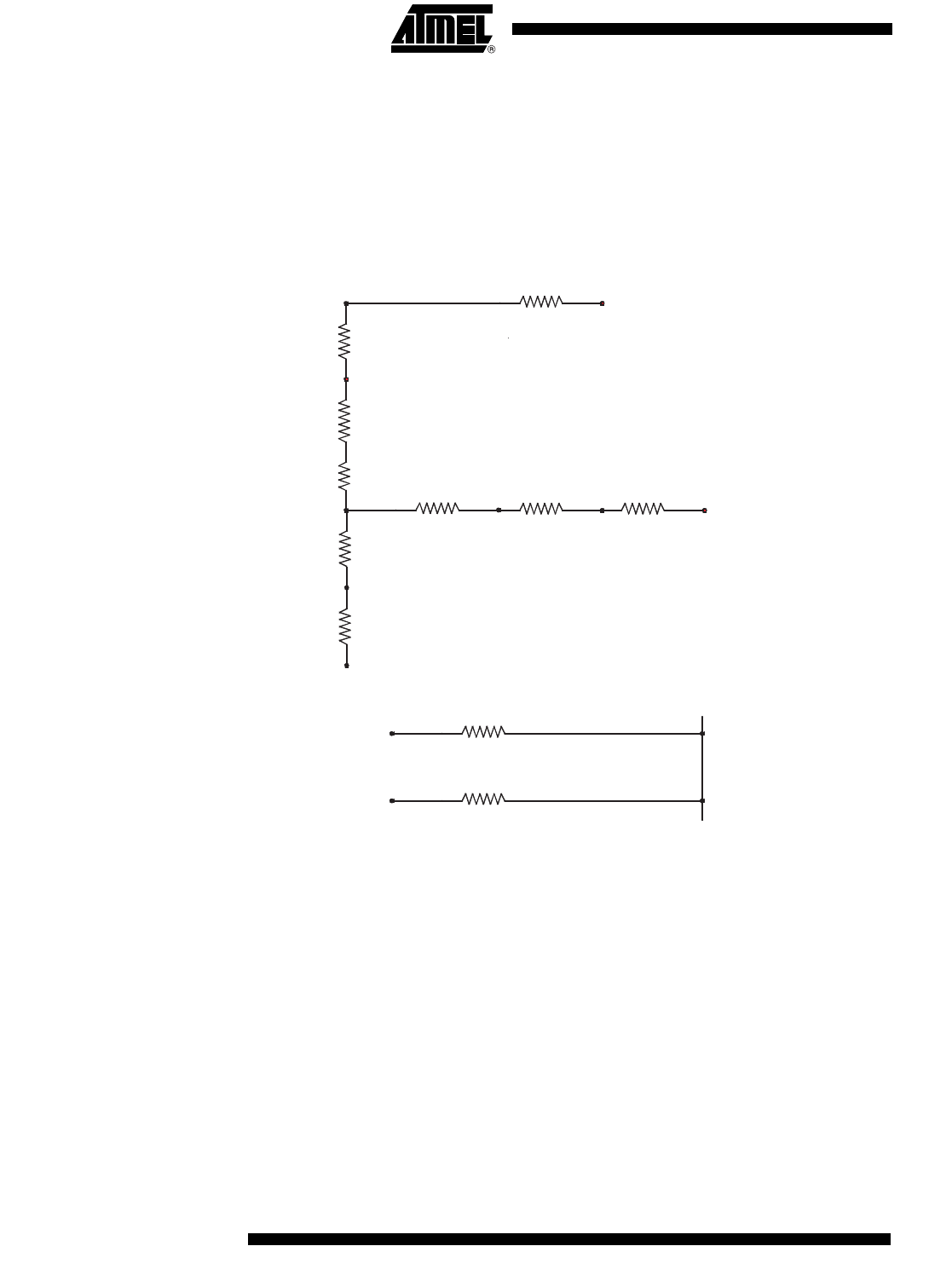
The following model has been extracted from the ANSYS FEM simulations.
Assumptions: no air, no convection and no board.
Figure 62. Simplified Thermal Model for LQFP Package
Note: The above are typical values with an assumption of uniform power dissipation over 2.5 x 2.5 mm
2
of the top surface of the die.
Thermal Resistance from
Junction to Bottom of Leads
Assumptions: no air, no convection and no board.
The thermal resistance from the junction to the bottom of the leads is 15.2° C/W typical.
Thermal Resistance from
Junction to Top of Case
Assumptions: no air, no convection and no board.
The thermal resistance from the junction to the top of the case is 8.3° C/W typical.
Thermal Resistance from
Junction to Bottom of Case
Assumptions: no air, no convection and no board.
The thermal resistance from the junction to the bottom of the case is 6.4° C/W typical.
Thermal Resistance from
Junction to Bottom of Air Gap
The thermal resistance from the junction to the bottom of the air gap (bottom of pack-
age) is 17.9° C/W typical.
355 µm silicon die
25 mm
λ
= 0.95W/cm/˚C
40 µm Epoxy/Ag glue
λ
= 0.02 W/cm/˚C
Copper paddle
λ
= 2.5W/cmC
Aluminium paddle
λ
= 0.75W/cm/˚C
Copper alloy leadframe
Package top
5.5˚C/watt
0.1˚C/watt
11.4˚C/watt
Package
bottom
4.3˚C/watt
1.5˚C/watt
λ
= 0.007W/cm/˚C
Silicon Junction
0.6˚C/watt
8.3˚C/watt
1.4˚C/watt
0.1˚C/watt
6.1˚C/watt
1.5˚C/watt
Leads tip
Assumptions:
Die 5.0 x 5.0 = 25 mm
40 µm thick Epoxy/Ag glue
2
Top of user board
Package bottom
connected to:
(user dependent)
Resin bottom
λ = 0.007W/cm/
˚C
2
Aluminium paddle Resin
Resin
λ
= 0.007W/cm/˚C
λ
= 25W/cm/˚C
100 µm air gap λ = 0.00027W/cm/
˚C
100 µm thermal grease gap diamater 12 mm
λ = 0.01W/cm/
˚C
57
AT84AD001B
2153C–BDC–04/04
Thermal Resistance from
Junction to Ambient
The thermal resistance from the junction to ambient is 25.2° C/W typical.
Note: In order to keep the ambient temperature of the die within the specified limits of the
device grade (that is T
A
max = 70°C in commercial grade and 85°C in industrial grade)
and the die junction temperature below the maximum allowed junction temperature of
105°C, it is necessary to operate the dual ADC in air flow conditions (1m/s recom-
mended).
In still air conditions, the junction temperature is indeed greater than the maximum
allowed T
J
.
- T
J
= 25.2°C/W x 1.4W + T
A
= 35.28 + 70 = 105.28°C for commercial grade devices
- T
J
= 25.2°C/W x 1.4W + T
A
= 35.28 + 85 = 125.28°C for industrial grade devices
Thermal Resistance from
Junction to Board
The thermal resistance from the junction to the board is 13° C/W typical.
PREVIOUS121314151617181920NEXT