Freelance Electronics Components Distributor
Closed Dec 25th-26th
800-300-1968
We Stock Hard to Find Parts

AT84AD001BITD

Part # AT84AD001BITD
Description ADC DUAL FLASH 1GSPS 8BIT PARALLEL 144LQFP - Trays
Category IC
Availability Out of Stock
Qty 0
Qty Price
1 + $154.41500


Technical Document


DISCLAIMER: The information provided herein is solely for informational purposes. Customers must be aware of the suitability of this product for their application, and consider that variable factors such as Manufacturer, Product Category, Date Codes, Pictures and Descriptions may differ from available inventory.

52
AT84AD001B
2153C–BDC–04/04
Figure 57. Termination Method for the ADC Analog Inputs in AC Coupling Mode
Clock Implementation The ADC features two different clocks (I or Q) that must be implemented as shown in
Figure 58. Each path must be AC coupled with a 100 nF capacitor.
Figure 58. Differential Termination Method for Clock I or Clock Q
Note: When only clock I is used, it is not necessary to add the capacitors on the CLKQ and
CLKQN signal paths; they may be left floating.
Channel I
Channel Q
50 Source
VinI
VinIB
VinQ
VinQB
VinI
VinIB
VinQ
VinQB
Dual ADC
50
50
50
50
GND
GND
50 Source
GND
GND
ADC Package
VCCD/2
50
50
100 nF
100 nF
Differential Buffer
CLK
CLKB
53
AT84AD001B
2153C–BDC–04/04
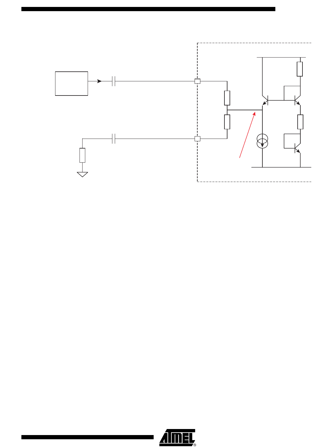
Figure 59. Single-ended Termination Method for Clock I or Clock Q
Output Termination in
1:1 Ratio
When using the integrated DMUX in 1:1 ratio, the valid port is port A. Port B remains
unused.
Port A functions in LVDS mode and the corresponding outputs (DOAI or DOAQ) have to
be 100 differentially terminated as shown in Figure 60 on page 54.
The pins corresponding to Port B (DOBI or DOBQ pins) must be left floating (in high
impedance state).
Figure 60 shows the example of a 1:1 ratio of the integrated DMUX for channel I (the
same applies to channel Q).
CLK
CLKB
50
50
VCCD
R1
R2
VCCD/2
AC coupling capacitor
50
Source
50
54
AT84AD001B
2153C–BDC–04/04
Figure 60. Example of Termination for Channel I Used in DMUX 1:1 Ratio (Port B Unused)
Note: If the outputs are to be used in single-ended mode, it is recommended that the true and false signals be terminated with a 50
resistor.
Using the Dual ADC With
and ASIC/FPGA Load
Figure 61 on page 55 illustrates the configuration of the dual ADC (1:2 DMUX mode,
independent I and Q clocks) driving an LVDS system (ASIC/FPGA) with potential addi-
tional DMUXes used to halve the speed of the dual ADC outputs.
Port B
DOBI0 / DOBI0N
DOBI1 / DOBI1N
DOBI2 / DOBI2N
DOBI3 / DOBI3N
DOBI4 / DOBI4N
DOBI5 / DOBI5N
DOBI6 / DOBI6N
DOBI7 / DOBI7N
Floating (High Z)
Port A
DOAI0 / DOAI0N
DOAI1 / DOAI1N
DOAI2 / DOAI2N
DOAI3 / DOAI3N
DOAI4 / DOAI4N
DOAI5 / DOAI5N
DOAI6 / DOAI6N
DOAI7 / DOAI7N
VCCO
DOAI0
DOAI0N
Z0 = 50
Z0 = 50
100
LVDS In
LVDS In
Dual ADC Package
PREVIOUS11121314151617181920NEXT