Freelance Electronics Components Distributor
Closed Dec 25th-26th
800-300-1968
We Stock Hard to Find Parts

AT84AD001BITD

Part # AT84AD001BITD
Description ADC DUAL FLASH 1GSPS 8BIT PARALLEL 144LQFP - Trays
Category IC
Availability Out of Stock
Qty 0
Qty Price
1 + $154.41500


Technical Document


DISCLAIMER: The information provided herein is solely for informational purposes. Customers must be aware of the suitability of this product for their application, and consider that variable factors such as Manufacturer, Product Category, Date Codes, Pictures and Descriptions may differ from available inventory.

49
AT84AD001B
2153C–BDC–04/04
TRDR Data Ready Reset
Delay
The delay between the falling edge of the Data Ready output asynchronous reset signal
(DDRB) and the reset to digital zero transition of the Data Ready output signal (DR)
TS Settling Time The time delay to rise from 10% to 90% of the converter output when a full-scale step
function is applied to the differential analog input
VSWR Voltage Standing
Wave Ratio
The VSWR corresponds to the ADC input insertion loss due to input power reflection. For
example, a VSWR of 1.2 corresponds to a 20 dB return loss (99% power transmitted and 1%
reflected)
Table 16. Definitions of Terms (Continued)
Abbreviation Definition Description
50
AT84AD001B
2153C–BDC–04/04
Using the AT84AD001B Dual 8-bit 1 Gsps ADC
Decoupling, Bypassing
and Grounding of Power
Supplies
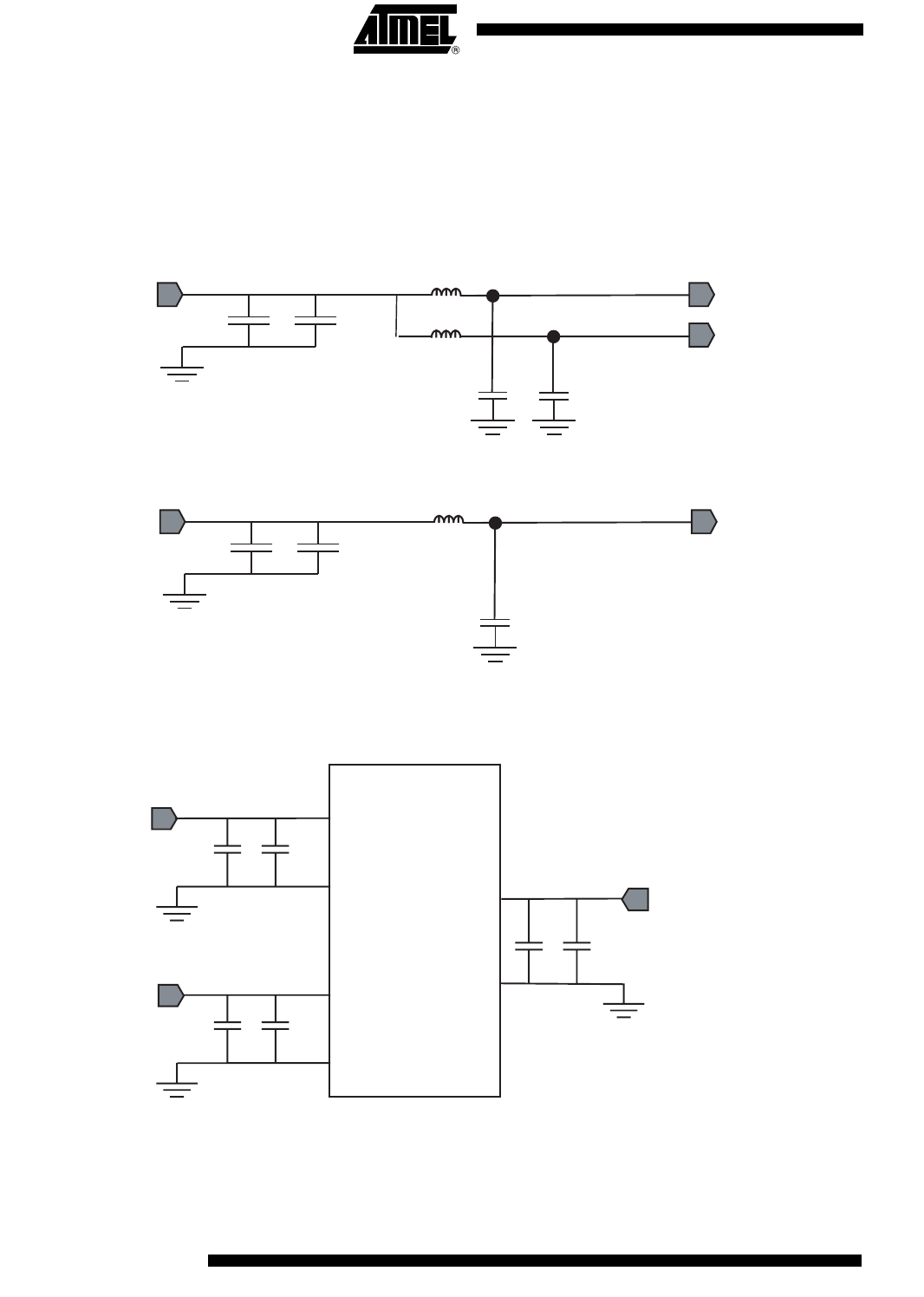
The following figures show the recommended bypassing, decoupling and grounding
schemes for the dual 8-bit 1 Gsps ADC power supplies.
Figure 53. V
CCD
and V
CCA
Bypassing and Grounding Scheme
Figure 54. V
CCO
Bypassing and Grounding Scheme
Note: L and C values must be chosen in accordance with the operation frequency of the application.
Figure 55. Power Supplies Decoupling Scheme
Note: The bypassing capacitors (1 µF and 100 pF) should be placed as close as possible to the board connectors, whereas the
decoupling capacitors (100 pF and 10 nF) should be placed as close as possible to the device.
1µF
L
PC Board 3.3V
PC Board GND
VCCD
L
C
C
VCCA
100 pF
1µF
L
PC Board 2.25V
PC Board GND
VCCO
C
100 pF
VCCA
GNDA
VCCO
GNDO
GNDA
GNDD
GNDO
VCCD
VCCA
VCCO
100 pF
100 pF 10 nF
10 nF
100 pF
10 nF
51
AT84AD001B
2153C–BDC–04/04
Analog Input
Implementation
The analog inputs of the dual ADC have been designed with a double pad implementa-
tion as illustrated in Figure 56. The reverse pad for each input should be tied to ground
via a 50 resistor.
The analog inputs must be used in differential mode only.
Figure 56. Termination Method for the ADC Analog Inputs in DC Coupling Mode
Channel I
Channel Q
50 Source
VinI
VinIB
VinQ
VinQB
VinI
VinIB
VinQ
VinQB
Dual ADC
50
50
50
50
GND
GND
50 Source
GND
GND
PREVIOUS1011121314151617181920NEXT