Freelance Electronics Components Distributor
Closed Dec 25th-26th
800-300-1968
We Stock Hard to Find Parts

AT84AD001BITD

Part # AT84AD001BITD
Description ADC DUAL FLASH 1GSPS 8BIT PARALLEL 144LQFP - Trays
Category IC
Availability Out of Stock
Qty 0
Qty Price
1 + $154.41500


Technical Document


DISCLAIMER: The information provided herein is solely for informational purposes. Customers must be aware of the suitability of this product for their application, and consider that variable factors such as Manufacturer, Product Category, Date Codes, Pictures and Descriptions may differ from available inventory.

40
AT84AD001B
2153C–BDC–04/04
Notes: 1. D9 must be set to “0”
2. Mode standby channel I: use analog input I Vini, Vinib and Clocki.
3. Mode standby channel Q: use analog input Q Vinq, Vinqb and Clockq.
4. Keep last calibration calculated value - no calibration phase: D11 = 0 and D10 = 1. No new calibration is required. The val-
ues taken into account for the gain and offset are either from the last calibration phase or are default values (reset values).
5. No calibration phase - no calibration value: D11 = 0 and D10 = 0. No new calibration phase is required. The gain and offset
compensation functions can be accessed externally by writing in the registers at address 010 for the offset compensation
and at address 011 for the gain compensation.
6. The control wait bit gives the possibility to change the internal setting for the auto-calibration phase:
For high clock rates (> 500 Msps) use a = b = 1.
For clock rates > 250 Msps and < 500 Msps use a = 1 and b = 0.
For clock rates > 125 Msps and < 250 Msps use a = 0 and b = 1.
For low clock rates < 125 Msps use a = 0 and b = 0.
3-wire Serial Interface Timing
Description
The 3-wire serial interface is a synchronous write-only serial interface made of three
wires:
sclk: serial clock input
sldn: serial load enable input
sdata: serial data input
The 3-wire serial interface gives write-only access to as many as 8 different internal reg-
isters of up to 16 bits each. The input format is always fixed with 3 bits of register
address followed by 16 bits of data. The data and address are entered with the Most
Significant Bit (MSB) first.
The write procedure is fully synchronous with the rising clock edge of “sclk” and
described in the write chronogram (Figure 44 on page 41).
“sldn” and “sdata” are sampled on each rising clock edge of “sclk” (clock cycle).
“sldn” must be set to 1 when no write procedure is performed.
A minimum of one rising clock edge (clock cycle) with “sldn” at 1 is required for a
correct start of the write procedure.
A write starts on the first clock cycle with “sldn” at 0. “sldn” must stay at 0 during the
complete write procedure.
During the first 3 clock cycles with “sldn” at 0, 3 bits of the register address from
MSB (a[2]) to LSB (a[0]) are entered.
During the next 16 clock cycles with “sldn” at 0, 16 bits of data from MSB (d[15]) to
LSB (d[0]) are entered.
An additional clock cycle with “sldn” at 0 is required for parallel transfer of the serial
data d[15:0] into the addressed register with address a[2:0]. This yields 20 clock
cycles with “sldn” at 0 for a normal write procedure.
Control wait bit
calibration
(6)
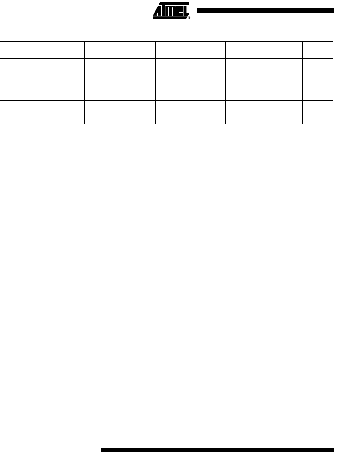
X X a b X X 0 XXXXXXXXX
In 1:2 DMUX
FDataReady
I & Q = Fs/2
X 0 X X X X 0 XXXXXXXXX
In 1:2 DMUX
FDataReady
I & Q = Fs/4
X 1 X X X X 0 XXXXXXXXX
Table 13. 3-wire Serial Interface Data Setting Description (Continued)
Setting for Address:
000 D15 D14 D13 D12 D11 D10 D9
(1)
D8 D7 D6 D5 D4 D3 D2 D1 D0
41
AT84AD001B
2153C–BDC–04/04
A minimum of one clock cycle with “sldn” returned at 1 is requested to close the
write procedure and make the interface ready for a new write procedure. Any clock
cycle where “sldn” is at 1 before the write procedure is completed interrupts this
procedure and no further data transfer to the internal registers is performed.
Additional clock cycles with “sldn” at 0 after the parallel data transfer to the register
(done at the 20th consecutive clock cycle with “sldn” at 0) do not affect the write
procedure and are ignored.
It is possible to have only one clock cycle with “sldn” at 1 between two following write
procedures.
16 bits of data must always be entered even if the internal addressed register has
less than 16 bits. Unused bits (usually MSBs) are ignored. Bit signification and bit
positions for the internal registers are detailed in Table 12 on page 37.
To reset the registers, the Pin mode can be used as a reset pin for chip initialization,
even when the 3-wire serial interface is used.
Figure 44. Write Chronogram
Figure 45. Timing Definition
Reset
Write procedure
a[2] a[1]
a[0] d[15]
d[8]
d[7]
d[6]
d[5]
d[4]
d[3]
d[2]
d[1]
d[0]
12 345 1314151617181920
Reset setting
Mode
sclk
sldn
sdata
Internal register
value
New d
Mode
sclk
sldn
sdata
Twlmode
Tdmode
Tssldn
Tssdata
Thsldn
Thsdata
Tdmode
Twsclk
Tsclk
42
AT84AD001B
2153C–BDC–04/04
Calibration Description The AT84AD001B offers the possibility of reducing offset and gain matching between
the two ADC cores. An internal digital calibration may start right after the 3-wire serial
interface has been loaded (using data D12 of the 3-wire serial interface with address
000).
The beginning of calibration disables the two ADCs and a standard data acquisition is
performed. The output bit CAL goes to a high level during the entire calibration phase.
When this bit returns to a low level, the two ADCs are calibrated with offset and gain and
can be used again for a standard data acquisition.
If only one channel is selected (I or Q) the offset calibration duration is divided by two
and no gain calibration between the two channels is necessary.
Figure 46. Internal Timing Calibration
The Tcal duration is a multiple of the clock frequency ClockI (master clock). Even if a
dual clock scheme is used during calibration, ClockQ will not be used.
The control wait bits (D13 and D14) give the possibility of changing the calibration’s set-
ting depending on the clock’s frequency:
For high clock rates (> 500 Msps) use a = b = 1, Tcal = 10112 clock I periods.
For clock rates > 250 Msps and < 500 Msps use a = 1, b = 0, Tcal = 6016 clock I
periods.
For clock rates > 125 Msps and < 250 Msps use a = 0, b = 1 ,Tcal = 3968 clock I
periods.
For low clock rates (< 125 Msps) use a = 0, b = 0 , Tcal = 2944 clock I periods.
Table 14. Timing Description
Name Parameter
Value
Unit
Min Typ Max
Tsclk Sclk period 20 ns
Twsclk High or low time of sclk 5 ns
Tssldn Setup time of sldn before rising edge of sclk 4 ns
Thsldn Hold time of sldn after rising edge of sclk 2 ns
Tssdata Setup time of sdata before rising edge of sclk 4 ns
Thsdata Hold time of sdata after rising edge of sclk 2 ns
Twlmode Minimum low pulse width of mode 5 ns
Tdmode
Minimum delay between an edge of mode and the
rising edge of sclk
10 ns
3-wire Serial Interface
LDN
CAL
Tcal
PREVIOUS7891011121314151617181920NEXT