Closed Dec 25th-26th
800-300-1968
We Stock Hard to Find Parts
My Account
|
My Orders
|
My Cart
Questions?
(800) 300-1968
Register
(current)
My Account
(current)
My Orders
(current)
My Cart
(current)
Categories
(current)
Manufacturers
Request a Quote
Sell Your Excess
Consignment
Quality Assurance
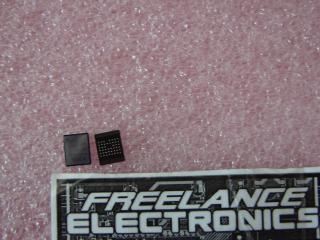
AT49BV163AT-70TU
Part #
AT49BV163AT-70TU
Description
IC FLASH 16MBIT 70NS 48TSOP
Category
IC
Availability
In Stock
Qty
22
Qty
Price
1 - 4
$5.81299
5 - 9
$4.62397
10 - 13
$4.35974
14 - 18
$4.05148
19 +
$3.61110
Manufacturer
Available
Qty
Atmel
Date Code: 0847
Freelance Stock:
22
Ships Immediately
Add to Cart
Related Items
Atmel
IC
AT49BV040-12JC
$5.30767
Atmel
IC
AT49BV1604-90UI
$19.74834
Atmel
IC
AT49BV322DT-70TU
$10.49314
Atmel
IC
AT49BV640DT-70CU
$37.36631
Fairchild Semiconductor
IC
008-25424
$11.58351
Harris Corporation
IC
01-6945-9