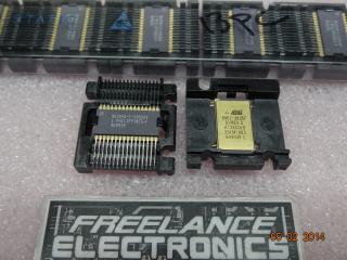
Freelance Electronics Components Distributor
Closed Dec 25th-26th
800-300-1968
We Stock Hard to Find Parts

AT28C64-12SC

Part # AT28C64-12SC
Description EEPROM Parallel 64K-bit 8K x8 5V 28-Pin SOIC
Category IC
Availability In Stock
Qty 43
Qty Price
1 - 9 $21.06217
10 - 18 $16.75400
19 - 27 $15.79663
28 - 36 $14.67969
37 + $13.08408
Manufacturer Available Qty
Atmel
Date Code: 0022
  • Shipping Freelance Stock: 30
    Ships Immediately
Atmel
Date Code: 0022
  • Shipping Freelance Stock: 13
    Ships Immediately


Technical Document


DISCLAIMER: The information provided herein is solely for informational purposes. Customers must be aware of the suitability of this product for their application, and consider that variable factors such as Manufacturer, Product Category, Date Codes, Pictures and Descriptions may differ from available inventory.

AT28C64/X
64K (8K x 8)
CMOS
E
2
PROM
Features
Fast Read Access Time - 120 ns
Fast Byte Write - 200 µs or 1 ms
Self-Timed Byte Write Cycle
Internal Address and Data Latches
Internal Control Timer
Automatic Clear Before Write
Direct Microprocessor Control
READY/BUSY Open Drain Output
DATA Polling
Low Power
30 mA Active Current
100 µA CMOS Standby Current
High Reliability
Endurance: 10
4
or 10
5
Cycles
Data Retention: 10 Years
5V ± 10% Supply
CMOS and TTL Compatible Inputs and Outputs
JEDEC Approved Byte-Wide Pinout
Commercial and Industrial Temperature Ranges
Description
The AT28C64 is a low-power, high-performance 8,192 words by 8 bit nonvolatile
Electrically Erasable and Programmable Read Only Memory with popular, easy to
use features. The device is manufactured with Atmel’s reliable nonvolatile technol-
ogy.
(continued)
PDIP, SOIC
Top View
Pin Name Function
A0 - A12 Addresses
CE Chip Enable
OE Output Enable
WE Write Enable
I/O0 - I/O7 Data Inputs/Outputs
RDY/
BUSY Ready/Busy Output
NC No Connect
DC Don’t Connect
Pin Configurations
TSOP
Top View
LCC, PLCC
Top View
Note: PLCC package pins 1 and
17 are DON’T CONNECT.
0001G
AT28C64/X
2-193
Description (Continued)
Block Diagram
The AT28C64 is accessed like a Static RAM for the read
or write cycles without the need for external components.
During a byte write, the address and data are latched in-
ternally, freeing the microprocessor address and data bus
for other operations. Following the initiation of a write cy-
cle, the device will go to a busy state and automatically
clear and write the latched data using an internal control
timer. The device includes two methods for detecting the
end of a write cycle, level detection of RDY/
BUSY (unless
pin 1 is N.C.) and
DATA POLLING of I/O
7
. Once the end
of a write cycle has been detected, a new access for a
read or write can begin.
The CMOS technology offers fast access times of 120 ns
at low power dissipation. When the chip is deselected the
standby current is less than 100 µA.
Atmel’s 28C64 has additional features to ensure high
quality and manufacturability. The device utilizes error cor-
rection internally for extended endurance and for im-
proved data retention characteristics. An extra 32-bytes of
E
2
PROM are available for device identification or tracking.
Temperature Under Bias................. -55°C to +125°C
Storage Temperature...................... -65°C to +150°C
All Input Voltages
(including NC Pins)
with Respect to Ground ................... -0.6V to +6.25V
All Output Voltages
with Respect to Ground .............-0.6V to V
CC
+ 0.6V
Voltage on
OE and A9
with Respect to Ground ................... -0.6V to +13.5V
*NOTICE: Stresses beyond those listed under “Absolute Maxi-
mum Ratings” may cause permanent damage to the device.
This is a stress rating only and functional operation of the
device at these or any other conditions beyond those indi-
cated in the operational sections of this specification is not
implied. Exposure to absolute maximum rating conditions
for extended periods may affect device reliability.
Absolute Maximum Ratings*
2-194 AT28C64/X
Device Operation
READ: The AT28C64 is accessed like a Static RAM.
When
CE and OE are low and WE is high, the data stored
at the memory location determined by the address pins is
asserted on the outputs. The outputs are put in a high im-
pedance state whenever
CE or OE is high. This dual line
control gives designers increased flexibility in preventing
bus contention.
BYTE WRITE: Writing data into the AT28C64 is similar to
writing into a Static RAM. A low pulse on the
WE or CE
input with
OE high and CE or WE low (respectively) initi-
ates a byte write. The address location is latched on the
falling edge of
WE (or CE); the new data is latched on the
rising edge. Internally, the device performs a self-clear be-
fore write. Once a byte write has been started, it will auto-
matically time itself to completion. Once a programming
operation has been initiated and for the duration of t
WC
, a
read operation will effectively be a polling operation.
FAST BYTE WRITE: The AT28C64E offers a byte write
time of 200 µs maximum. This feature allows the entire
device to be rewritten in 1.6 seconds.
READY/
BUSY: Pin 1 is an open drain READY/BUSY
output that can be used to detect the end of a write cycle.
RDY/
BUSY is actively pulled low during the write cycle
and is released at the completion of the write. The open
drain connection allows for OR-tying of several devices to
the same RDY/
BUSY line. Pin 1 is not connected for the
AT28C64X.
DATA POLLING: The AT28C64 provides DATA POLL-
ING to signal the completion of a write cycle. During a
write cycle, an attempted read of the data being written
results in the complement of that data for I/O
7
(the other
outputs are indeterminate). When the write cycle is fin-
ished, true data appears on all outputs.
WRITE PROTECTION: Inadvertent writes to the device
are protected against in the following ways. (a) V
CC
sense— if V
CC
is below 3.8V (typical) the write function is
inhibited. (b) V
CC
power on delay— once V
CC
has
reached 3.8V the device will automatically time out 5 ms
(typical) before allowing a byte write. (c) Write Inhibit—
holding any one of
OE low, CE high or WE high inhibits
byte write cycles.
CHIP CLEAR: The contents of the entire memory of the
AT28C64 may be set to the high state by the CHIP CLEAR
operation. By setting
CE low and OE to 12 volts, the chip
is cleared when a 10 msec low pulse is applied to
WE.
DEVICE IDENTIFICATION: An extra 32-bytes of
E
2
PROM memory are available to the user for device
identification. By raising A9 to 12 ± 0.5V and using ad-
dress locations 1FE0H to 1FFFH the additional bytes may
be written to or read from in the same manner as the regu-
lar memory array.
AT28C64/X
2-195
1234NEXT