Closed Dec 25th-26th
800-300-1968
We Stock Hard to Find Parts
My Account
|
My Orders
|
My Cart
Questions?
(800) 300-1968
Register
(current)
My Account
(current)
My Orders
(current)
My Cart
(current)
Categories
(current)
Manufacturers
Request a Quote
Sell Your Excess
Consignment
Quality Assurance
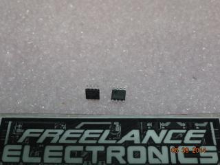
AT25640N-10SI
Part #
AT25640N-10SI
Description
IC EEPROM 64KBIT 3MHZ 8SOIC
Category
IC
Availability
Out of Stock
Qty
0
Qty
Price
1 +
$2.12000
Related Items
Atmel
IC
AT25640AN-10SI-2.7
$0.39413
Atmel
IC
AT25640N-10SC
$1.50169
Fairchild Semiconductor
IC
008-25424
$11.58351
Harris Corporation
IC
01-6945-9
Motorola Corp
IC
010-143121-0002
Texas Instruments
IC
01295-672141D