Closed Dec 25th-26th
800-300-1968
We Stock Hard to Find Parts
My Account
|
My Orders
|
My Cart
Questions?
(800) 300-1968
Register
(current)
My Account
(current)
My Orders
(current)
My Cart
(current)
Categories
(current)
Manufacturers
Request a Quote
Sell Your Excess
Consignment
Quality Assurance
AM26LV31INSR
Part #
AM26LV31INSR
Description
IC QUAD DIFF LINE DVR HS 16SO
Category
IC
Availability
In Stock
Qty
105
Qty
Price
1 - 22
$0.45903
23 - 44
$0.36514
45 - 66
$0.34427
67 - 88
$0.31993
89 +
$0.28516
Manufacturer
Available
Qty
Texas Instruments
Date Code: 0640
Freelance Stock:
97
Ships Immediately
Texas Instruments
Freelance Stock:
8
Ships Immediately
Add to Cart
Related Items
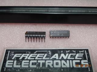
Advanced Micro Devices
IC
AM26L02DMB
$23.19215
Advanced Micro Devices
IC
AM26L31DC
$4.28592
Advanced Micro Devices
IC
AM26L32BPC
$31.09964
Advanced Micro Devices
IC
AM26LS29/BEA
$10.04510
Analog Devices
IC
AM26LS29DC
$20.21476
Advanced Micro Devices
IC
AM26LS29PC
$3.29317