ProASIC3 DC and Switching Characteristics
v1.3 2-91
Timing Characteristics
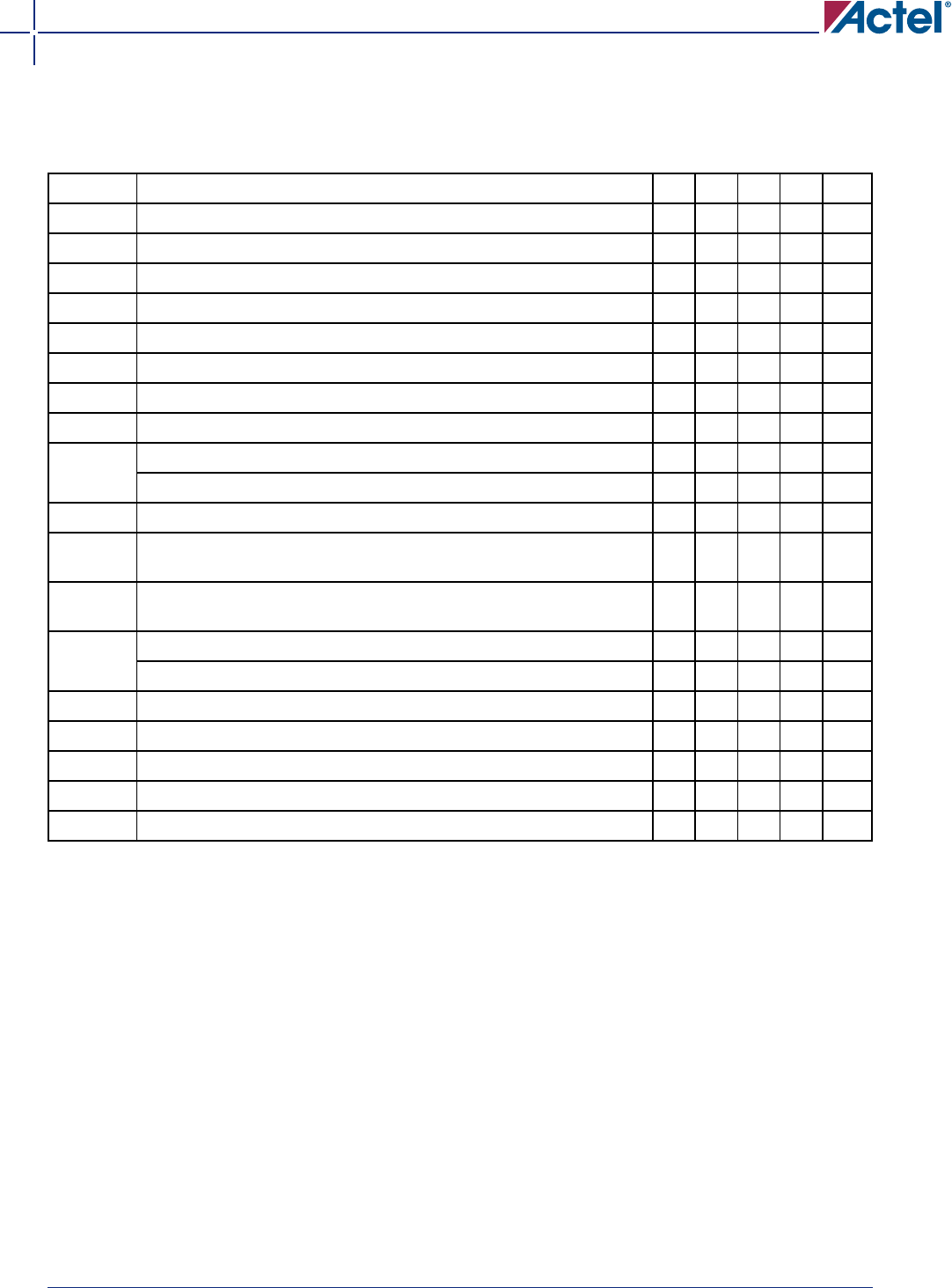
Table 2-107 • RAM4K9
Commercial-Case Conditions: T
J
= 70°C, Worst-Case V
CC
= 1.425 V
Parameter Description –2 –1 Std. –F Units
t
AS
Address setup time 0.25 0.28 0.33 0.40 ns
t
AH
Address hold time 0.00 0.00 0.00 0.00 ns
t
ENS
REN_B, WEN_B setup time 0.14 0.16 0.19 0.23 ns
t
ENH
REN_B, WEN_B hold time 0.10 0.11 0.13 0.16 ns
t
BKS
BLK_B setup time 0.23 0.27 0.31 0.37 ns
t
BKH
BLK_B hold time 0.02 0.02 0.02 0.03 ns
t
DS
Input data (DI) setup time 0.18 0.21 0.25 0.29 ns
t
DH
Input data (DI) hold time 0.00 0.00 0.00 0.00 ns
t
CKQ1
Clock HIGH to new data valid on DO (output retained, WMODE = 0) 2.36 2.68 3.15 3.79 ns
Clock HIGH to new data valid on DO (flow-through, WMODE = 1) 1.79 2.03 2.39 2.87 ns
t
CKQ2
Clock HIGH to new data valid on DO (pipelined) 0.89 1.02 1.20 1.44 ns
t
WRO
Address collision clk-to-clk delay for reliable read access after write
on same address
TBDTBDTBDTBD ns
t
CCKH
Address collision clk-to-clk delay for reliable write access after
write/read on same address
TBDTBDTBDTBD ns
t
RSTBQ
RESET_B LOW to data out LOW on DO (flow-through) 0.92 1.05 1.23 1.48 ns
RESET_B LOW to Data Out LOW on DO (pipelined) 0.92 1.05 1.23 1.48 ns
t
REMRSTB
RESET_B removal 0.29 0.33 0.38 0.46 ns
t
RECRSTB
RESET_B recovery 1.50 1.71 2.01 2.41 ns
t
MPWRSTB
RESET_B minimum pulse width 0.21 0.24 0.29 0.34 ns
t
CYC
Clock cycle time 3.23 3.68 4.32 5.19 ns
F
MAX
Maximum frequency 310 272 231 193 MHz
Note: For specific junction temperature and voltage supply levels, refer to Table 2-6 on page 2-6 for derating
values.


