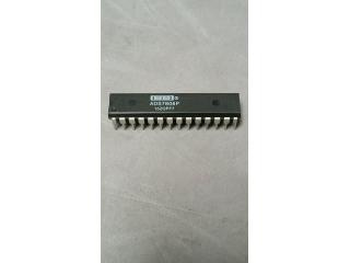
Freelance Electronics Components Distributor
Closed Dec 25th-26th
800-300-1968
We Stock Hard to Find Parts

ADS7844N

Part # ADS7844N
Description A/D CONV, 8-CHANNEL, 12 BIT SAMPLING - Rail/Tube
Category IC
Availability In Stock
Qty 72
Qty Price
1 - 3 $48.00000
4 - 7 $38.40000
8 - 17 $31.68000
18 - 26 $29.44000
27 + $26.24000
Manufacturer Available Qty
Burr-Brown Corporation
Date Code: 0034
  • Shipping Freelance Stock: 2
    Ships Immediately
Burr-Brown Corporation
  • Shipping Freelance Stock: 70
    Ships Immediately


Technical Document


DISCLAIMER: The information provided herein is solely for informational purposes. Customers must be aware of the suitability of this product for their application, and consider that variable factors such as Manufacturer, Product Category, Date Codes, Pictures and Descriptions may differ from available inventory.

ADS7844
12-Bit, 8-Channel Serial Output Sampling
ANALOG-TO-DIGITAL CONVERTER
FEATURES
SINGLE SUPPLY: 2.7V to 5V
8-CHANNEL SINGLE-ENDED OR
4-CHANNEL DIFFERENTIAL INPUT
UP TO 200kHz CONVERSION RATE
±1 LSB MAX INL AND DNL
NO MISSING CODES
72dB SINAD
SERIAL INTERFACE
20-LEAD QSOP AND
20-LEAD SSOP PACKAGES
ALTERNATE SOURCE FOR MAX147
DESCRIPTION
The ADS7844 is an 8-channel, 12-bit sampling analog-to-
digital converter (ADC) with a synchronous serial interface.
Typical power dissipation is 3mW at a 200kHz throughput
rate and a +5V supply. The reference voltage (V
REF
) can be
varied between 100mV and V
CC
, providing a corresponding
input voltage range of 0V to V
REF
. The device includes a
shutdown mode that reduces power dissipation to under
1µW. The ADS7844 is ensured down to 2.7V operation.
Low power, high speed, and onboard multiplexer make the
ADS7844 ideal for battery-operated systems such as personal
digital assistants, portable multichannel data loggers, and
measurement equipment. The serial interface also provides
low-cost isolation for remote data acquisition. The ADS7844
is available in a 20-lead QSOP package and the MAX147
equivalent 20-lead SSOP package and is ensured over the
–40°C to +85°C temperature range.
APPLICATIONS
DATA ACQUISITION
TEST AND MEASUREMENT
INDUSTRIAL PROCESS CONTROL
PERSONAL DIGITAL ASSISTANTS
BATTERY-POWERED SYSTEMS
CDAC
SAR
Comparator
Eight
Channel
Multiplexer
Serial
Interface
and
Control
CH4
CH5
CH6
CH7
COM
V
REF
CH0
CH1
CH2
CH3
CS
SHDN
DIN
DOUT
BUSY
DCLK
A
D
S
7
8
4
4
ADS7844
SBAS100A – JANUARY 1998 – REVISED OCTOBER 2003
www.ti.com
PRODUCTION DATA information is current as of publication date.
Products conform to specifications per the terms of Texas Instruments
standard warranty. Production processing does not necessarily include
testing of all parameters.
Copyright © 1998-2003, Texas Instruments Incorporated
Please be aware that an important notice concerning availability, standard warranty, and use in critical applications of
Texas Instruments semiconductor products and disclaimers thereto appears at the end of this data sheet.
All trademarks are the property of their respective owners.
ADS7844
2
SBAS100A
www.ti.com
SPECIFICATION: +5V
At T
A
= –40°C to +85°C, +V
CC
= +5V, V
REF
= +5V, f
SAMPLE
= 200kHz, and f
CLK
= 16 • f
SAMPLE
= 3.2MHz, unless otherwise noted.
ADS7844E, N ADS7844EB, NB
PARAMETER CONDITIONS MIN TYP MAX MIN TYP MAX UNITS
ANALOG INPUT
Full-Scale Input Span Positive Input - Negative Input 0 V
REF
✻✻V
Absolute Input Range Positive Input –0.2 +V
CC
+0.2 ✻✻V
Negative Input –0.2 +1.25 ✻✻V
Capacitance 25 pF
Leakage Current ±1 µA
SYSTEM PERFORMANCE
Resolution 12 Bits
No Missing Codes 12 Bits
Integral Linearity Error ±2 ±1 LSB
(1)
Differential Linearity Error ±0.8 ±0.5 ±1 LSB
Offset Error ±3 LSB
Offset Error Match 0.15 1.0 ✻✻ LSB
Gain Error ±4 ±3 LSB
Gain Error Match 0.1 1.0 ✻✻ LSB
Noise 30 µVrms
Power Supply Rejection 70 dB
SAMPLING DYNAMICS
Conversion Time 12 Clk Cycles
Acquisition Time 3 Clk Cycles
Throughput Rate 200 kHz
Multiplexer Settling Time 500 ns
Aperture Delay 30 ns
Aperture Jitter 100 ps
DYNAMIC CHARACTERISTICS
Total Harmonic Distortion
(2)
V
IN
= 5V
PP
at 10kHz –76 –78 dB
Signal-to-(Noise + Distortion) V
IN
= 5V
PP
at 10kHz 71 72 dB
Spurious Free Dynamic Range V
IN
= 5V
PP
at 10kHz 76 78 dB
Channel-to-Channel Isolation V
IN
= 5V
PP
at 50kHz 120 dB
REFERENCE INPUT
Range 0.1 +V
CC
✻✻V
Resistance DCLK Static 5 G
Input Current 45 100 ✻✻ µA
f
SAMPLE
= 12.5kHz 2.5 µA
DCLK Static 0.001 3 ✻✻ µA
DIGITAL INPUT/OUTPUT
Logic Family CMOS
Logic Levels
V
IH
| I
IH
| +5µA 3.0 5.5 ✻✻V
V
IL
| I
IL
| +5µA –0.3 +0.8 ✻✻V
V
OH
I
OH
= –250µA 3.5 V
V
OL
I
OL
= 250µA 0.4 V
Data Format Straight Binary
POWER SUPPLY REQUIREMENTS
+V
CC
Specified Performance 4.75 5.25 ✻✻V
Quiescent Current 550 900 µA
f
SAMPLE
= 12.5kHz 300 µA
Power-Down Mode
(3)
, CS = +V
CC
3 µA
Power Dissipation 4.5 mW
TEMPERATURE RANGE
Specified Performance –40 +85 ✻✻°C
Same specifications as ADS7844E, ADS7844N.
NOTE: (1) LSB means Least Significant Bit. With V
REF
equal to +5.0V, one LSB is 1.22mV. (2) First five harmonics of the test frequency. (3) Auto power-down mode
(PD1 = PD0 = 0) active or SHDN = GND.
ADS7844
3
SBAS100A
www.ti.com
SPECIFICATION: +2.7V
At T
A
= –40°C to +85°C, +V
CC
= +2.7V, V
REF
= +2.5V, f
SAMPLE
= 125kHz, and f
CLK
= 16 • f
SAMPLE
= 2MHz, unless otherwise noted.
ADS7844E, N ADS7844EB, NB
PARAMETER CONDITIONS MIN TYP MAX MIN TYP MAX UNITS
ANALOG INPUT
Full-Scale Input Span Positive Input - Negative Input 0 V
REF
✻✻V
Absolute Input Range Positive Input –0.2 +V
CC
+0.2 ✻✻V
Negative Input –0.2 +0.2 ✻✻V
Capacitance 25 pF
Leakage Current ±1 µA
SYSTEM PERFORMANCE
Resolution 12 Bits
No Missing Codes 12 Bits
Integral Linearity Error ±2 ±1 LSB
(1)
Differential Linearity Error ±0.8 ±0.5 ±1 LSB
Offset Error ±3 LSB
Offset Error Match 0.15 1.0 ✻✻ LSB
Gain Error ±4 ±3 LSB
Gain Error Match 0.1 1.0 ✻✻ LSB
Noise 30 µVrms
Power Supply Rejection 70 dB
SAMPLING DYNAMICS
Conversion Time 12 Clk Cycles
Acquisition Time 3 Clk Cycles
Throughput Rate 125 kHz
Multiplexer Settling Time 500 ns
Aperture Delay 30 ns
Aperture Jitter 100 ps
DYNAMIC CHARACTERISTICS
Total Harmonic Distortion
(2)
V
IN
= 2.5V
PP
at 10kHz –75 –77 dB
Signal-to-(Noise + Distortion) V
IN
= 2.5V
PP
at 10kHz 71 72 dB
Spurious Free Dynamic Range V
IN
= 2.5V
PP
at 10kHz 78 80 dB
Channel-to-Channel Isolation V
IN
= 2.5V
PP
at 50kHz 100 dB
REFERENCE INPUT
Range 0.1 +V
CC
✻✻V
Resistance DCLK Static 5 G
Input Current 13 40 ✻✻ µA
f
SAMPLE
= 12.5kHz 2.5 µA
DCLK Static 0.001 3 ✻✻ µA
DIGITAL INPUT/OUTPUT
Logic Family CMOS
Logic Levels
V
IH
| I
IH
| +5µA+V
CC
• 0.7 5.5 ✻✻V
V
IL
| I
IL
| +5µA –0.3 +0.8 ✻✻V
V
OH
I
OH
= –250µA+V
CC
• 0.8 V
V
OL
I
OL
= 250µA 0.4 V
Data Format Straight Binary
POWER SUPPLY REQUIREMENTS
+V
CC
Specified Performance 2.7 3.6 ✻✻V
Quiescent Current 280 650 ✻✻ µA
f
SAMPLE
= 12.5kHz 220 µA
Power-Down Mode
(3)
, CS = +V
CC
3 µA
Power Dissipation 1.8 mW
TEMPERATURE RANGE
Specified Performance –40 +85 ✻✻°C
Same specifications as ADS7844E, ADS7844N.
NOTE: (1) LSB means Least Significant Bit. With V
REF
equal to +2.5V, one LSB is 610mV. (2) First five harmonics of the test frequency. (3) Auto power-down mode
(PD1 = PD0 = 0) active or SHDN = GND.
1234567NEXT