Closed Dec 25th-26th
800-300-1968
We Stock Hard to Find Parts
My Account
|
My Orders
|
My Cart
Questions?
(800) 300-1968
Register
(current)
My Account
(current)
My Orders
(current)
My Cart
(current)
Categories
(current)
Manufacturers
Request a Quote
Sell Your Excess
Consignment
Quality Assurance
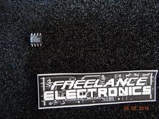
ADR03
Part #
ADR03
Description
Category
IC
Availability
Out of Stock
Qty
0
Related Items
Analog Devices
IC
ADR03A
Analog Devices
IC
ADR03AKSZ-REEL7
$1.08914
Analog Devices
IC
ADR03AR
$1.66077
Fairchild Semiconductor
IC
008-25424
$11.58351
Harris Corporation
IC
01-6945-9
Motorola Corp
IC
010-143121-0002