ADG608/ADG609
REV. A
–5–
ABSOLUTE MAXIMUM RATINGS
1
(T
A
= +25°C unless otherwise noted)
V
DD
to V
SS
. . . . . . . . . . . . . . . . . . . . . . . . . . . . . . . . . . +13 V
V
DD
to GND . . . . . . . . . . . . . . . . . . . . . . . . . –0.3 V to +6.5 V
V
SS
to GND . . . . . . . . . . . . . . . . . . . . . . . . . +0.3 V to –6.5 V
Analog, Digital Inputs
2
. . . . . . . . . . . . . . –0.3 V to V
DD
+ 2 V
or 20 mA, Whichever Occurs First
Continuous Current, S or D . . . . . . . . . . . . . . . . . . . . 20 mA
Peak Current, S or D
(Pulsed at 1 ms, 10% Duty Cycle Max) . . . . . . . . . . 40 mA
Operating Temperature Range
Industrial (B Version) . . . . . . . . . . . . . . . . –40°C to +85°C
Extended (T Version) . . . . . . . . . . . . . . . –55°C to +125°C
Storage Temperature Range . . . . . . . . . . . . –65°C to +150°C
Junction Temperature . . . . . . . . . . . . . . . . . . . . . . . . +150°C
Plastic DIP Package
θ
JA
, Thermal Impedance . . . . . . . . . . . . . . . . . . . . 117°C/W
Lead Temperature, Soldering (10 sec) . . . . . . . . . . +260°C
SOIC Package
θ
JA
, Thermal Impedance . . . . . . . . . . . . . . . . . . . . . . 77°C/W
Lead Temperature, Soldering
Vapor Phase (60 sec) . . . . . . . . . . . . . . . . . . . . . . +215°C
Infrared (15 sec) . . . . . . . . . . . . . . . . . . . . . . . . . . +220°C
TSSOP Package
θ
JA
, Thermal Impedance . . . . . . . . . . . . . . . . . . . . . 158°C/W
Lead Temperature, Soldering
Vapor Phase (60 sec) . . . . . . . . . . . . . . . . . . . . . . +215°C
Infrared (15 sec) . . . . . . . . . . . . . . . . . . . . . . . . . . +220°C
ESD Rating . . . . . . . . . . . . . . . . . . . . . . . . . . . . . . . . >5000 V
NOTES
1
Stresses above those listed under “Absolute Maximum Ratings” may cause
permanent damage to the device. This is a stress rating only and functional
operation of the device at these or any other conditions above those listed in the
operational sections of this specification is not implied. Exposure to absolute
maximum rating conditions for extended periods may affect device reliability.
Only one absolute maximum rating may be applied at any one time.
2
Overvoltages at A, S, D or EN will be clamped by internal diodes. Current should
be limited to the maximum ratings given.
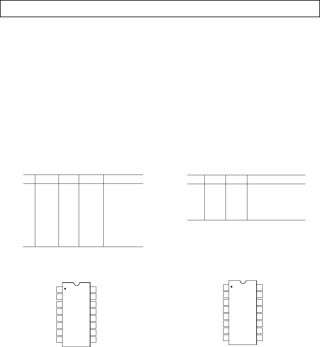
PIN CONFIGURATIONS
DIP/SOIC/TSSOP
DIP/SOIC/TSSOP
A0
EN
A1
GND
S2A
S3A
S4A
S2B
S3B
S4B
V
SS
S1A
V
DD
S1B
DA
DB
1
2
16
15
5
6
7
12
11
10
3
4
14
13
8
9
TOP VIEW
(Not to Scale)
ADG609
A0
EN
S2
S3
S4
V
SS
S1
D
1
2
16
15
5
6
7
12
11
10
3
4
14
13
8
9
TOP VIEW
(Not to Scale)
ADG608
A1
A2
S5
S6
S7
GND
V
DD
S8
Table I. ADG608 Truth Table
A2 A1 A0 EN ON SWITCH
X X X 0 NONE
00 0 1 1
00 1 1 2
01 0 1 3
01 1 1 4
10 0 1 5
10 1 1 6
11 0 1 7
11 1 1 8
X = Don’t Care
Table II. ADG609 Truth Table
A1 A0 EN ON SWITCH PAIR
X X 0 NONE
00 1 1
01 1 2
10 1 3
11 1 4
X = Don’t Care


