Closed Dec 25th-26th
800-300-1968
We Stock Hard to Find Parts
My Account
|
My Orders
|
My Cart
Questions?
(800) 300-1968
Register
(current)
My Account
(current)
My Orders
(current)
My Cart
(current)
Categories
(current)
Manufacturers
Request a Quote
Sell Your Excess
Consignment
Quality Assurance
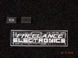
ADG438FBR
Part #
ADG438FBR
Description
ANLG MUX SGL 8:1 25V/25V 16SOIC N - Rail/Tube
Category
IC
Availability
Out of Stock
Qty
0
Qty
Price
1 +
$4.74105
Related Items
Analog Devices
IC
ADG431BN
$3.68929
Analog Devices
IC
ADG431BR
$8.56581
Analog Devices
IC
ADG433BR
$4.26974
Analog Devices
IC
ADG436BR
$4.64920
Analog Devices
IC
ADG438FBN
$3.71074
Fairchild Semiconductor
IC
008-25424
$11.58351