AD9696/AD9698
–7–
REV. B
2
AD9696
–IN
+IN
+V
S
1– 40MHz
LATCH
ENABLE
+
–
OSCILLATOR
OUTPUT
GROUND
Q
OUT
2kΩ
+V
S
0.1µF
(220pF for Freq. > 10MHz)
0.1µF
FOR USE WITH
OVERTONE
CRYSTAL
(VALUE
DEPENDS
ON FREQ.)
3
1 5
7
8
4
6
2kΩ
2kΩ
Q
OUT
–V
S
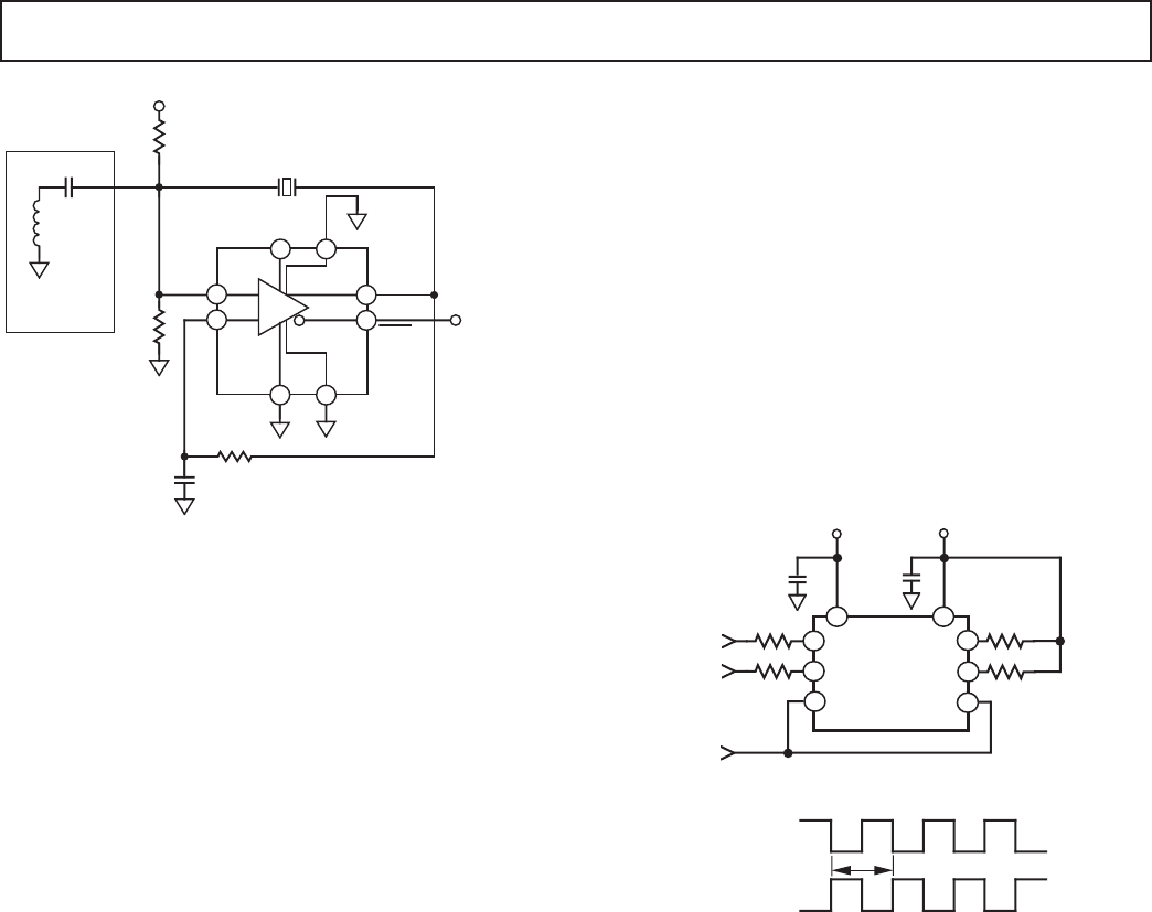
Figure 2. AD9696 Oscillator Circuit (Based on DIP Pinouts)
When generating frequencies using a nonfundamental mode
crystal, a choke and dc blocking capacitor are added. As an ex-
ample, a 36 MHz oscillator can be achieved by using a 12 MHz
crystal operating on its third overtone. To suppress oscillation at
the 12 MHz fundamental, the value of the choke is chosen to
provide a low reactive impedance at the fundamental frequency
while maintaining a high reactive impedance at the desired out-
put frequency (for 36 MHz operation, L = 1.8 µH). The shunt
capacitor at the inverting input has a value of 220 pF for a stable
36 MHz frequency.
LAYOUT CONSIDERATIONS
When working with high speed circuits, proper layout is critical.
Analog signal paths should be kept as short as possible and be
properly terminated to avoid reflections. In addition, digital sig-
nal paths should be kept short, and run lengths should be mat-
ched to avoid propagation delay mismatch. All analog signals
should be kept as far away from digital signal paths as possible;
this reduces the amount of digital switching noise that might be
capacitively coupled into the analog section of the circuit.
In high speed circuits, layout of the ground circuit is the most
important factor. A single, low impedance ground plane, on the
component side of the board, will reduce noise in the circuit
ground. It is especially important to maintain continuity of the
ground plane under and around the AD9696 or AD9698.
Sockets limit the dynamic performance of the device and should
be used only for prototypes or evaluation.
8
7
6
5
4
3
2
1
AD9696
(8-PIN DIP)
0.1µF
0.1µF
AD1
AD2
GND
RESISTORS ARE 1kΩ ±5%
– V
S
+V
S
5µs
–0.9V
AD1
AD2
–0.9 V
–1.7V
–1.7V
Burn-In Circuit