Freelance Electronics Components Distributor
Closed Dec 25th-26th
800-300-1968
We Stock Hard to Find Parts

AD9698KN

Part # AD9698KN
Description
Category IC
Availability In Stock
Qty 39
Qty Price
1 - 8 $30.61364
9 - 16 $24.35176
17 - 24 $22.96023
25 - 32 $21.33678
33 + $19.01756
Manufacturer Available Qty
Analog Devices
Date Code: 9600
  • Shipping Freelance Stock: 30
    Ships Immediately
Analog Devices
Date Code: 9604
  • Shipping Freelance Stock: 9
    Ships Immediately


Technical Document


DISCLAIMER: The information provided herein is solely for informational purposes. Customers must be aware of the suitability of this product for their application, and consider that variable factors such as Manufacturer, Product Category, Date Codes, Pictures and Descriptions may differ from available inventory.

AD9696/AD9698
–4–
REV. B
PIN CONFIGURATIONS
AD9696KN/KR/KQ/TQ/TZ
Q1
OUT
(N/C)
Q1
OUT
(–V
S
)
GROUND (–IN
1
)
LATCH ENABLE 1 (+IN
1
)
N/C (+IN
2
)
–V
S
(–IN
2
)
–IN
1
(+V
S
)
TOP VIEW
(Not to Scale)
1
2
3
4
5
6
7
8
9
10
11
12
13
14
16
15
+IN
1
(N/C)
+IN
2
(LATCH ENABLE 2)
–IN
2
(GROUND)
N/C (Q2
OUT
)
LATCH ENABLE 2 (Q1
OUT
)
Q2
OUT
(GROUND)
Q2
OUT
(LATCH ENABLE 1)
AD9698KN/KQ/TQ
[AD9698KR/TZ PINOUTS SHOWN IN ( )]
GROUND (Q1
OUT
)
+V
S
(Q2
OUT
)
LATCH
ENABLE
1
2
3
4
TOP VIEW
(Not to Scale)
5
6
7
8
+V
S
+IN
–IN
–V
S
GROUND
Q
OUT
Q
OUT
Name Function
Q1
OUT
One of two complementary outputs. Q1
OUT
will be at logic HIGH if voltage at +IN
1
is greater than voltage at
–IN
1
and LATCH ENABLE 1 is at logic LOW.
Q1
OUT
One of two complementary outputs. Q1
OUT
will be at logic HIGH if voltage at –IN
1
is greater than voltage at
+IN
1
and LATCH ENABLE 1 is at logic LOW.
GROUND Analog and digital ground return. All GROUND pins should be connected together and to a low impedance
ground plane near the comparator.
LATCH Output at Q1
OUT
will track differential changes at the inputs when LATCH ENABLE 1 is at logic LOW.
ENABLE 1 When LATCH ENABLE 1 is at logic HIGH, the output at Q1
OUT
will reflect the input state at the application of
the latch command, delayed by the Latch Enable Setup Time (t
S
). Since the architecture of the input stage (see
block diagram) is faster than the logic of the latch stage, data will typically be latched if applied to the comparator(s)
within 1.7 ns after the latch. This is the Setup Time (t
S
); for guaranteed performance, t
S
must be 3 ns.
N/C No internal connection to comparator.
–V
S
Negative power supply connection; nominally –5.2 V.
–IN
1
Inverting input of differential input stage for Comparator #1.
+IN
1
Noninverting input of differential input stage for Comparator #1.
+IN
2
Noninverting input of differential input stage for Comparator #2.
–IN
2
Inverting input of differential input stage for Comparator #2.
+V
S
Positive power supply connection; nominally +5 V.
LATCH Output at Q2
OUT
will track differential changes at the inputs when LATCH ENABLE 2 is at logic LOW.
ENABLE 2 When LATCH ENABLE 2 is at logic HIGH, the output at Q2
OUT
will reflect the input state at the application of
the latch command, delayed by the Latch Enable Setup Time (t
S
). Since the architecture of the input stage (see
block diagram) is faster than the logic of the latch stage, data will typically be latched if applied to the comparator(s)
within 1.7 ns after the latch. This is the Setup Time (t
S
); for guaranteed performance, t
S
must be 3 ns.
Q2
OUT
One of two complementary outputs. Q2
OUT
will be at logic HIGH if voltage at –IN
2
is greater than voltage at
+IN
2
and LATCH ENABLE 2 is at logic LOW.
Q2
OUT
One of two complementary outputs. Q2
OUT
will be at logic HIGH if voltage at +IN
2
is greater than voltage at
–IN
2
and LATCH ENABLE 2 is at logic LOW.
WARNING!
ESD SENSITIVE DEVICE
CAUTION
ESD (electrostatic discharge) sensitive device. Electrostatic charges as high as 4000 V readily
accumulate on the human body and test equipment and can discharge without detection.
Although the AD9696/AD9698 features proprietary ESD protection circuitry, permanent dam-
age may occur on devices subjected to high energy electrostatic discharges. Therefore, proper
ESD precautions are recommended to avoid performance degradation or loss of functionality.
AD9696/AD9698
–5–
REV. B
t
H
50%
50%
LATCH
ENABLE
DIFFERENTIAL
INPUT VOLTAGE
Q
TWO DIODES
ABOVE GROUND
LATCH
COMPARE
Q
t
PD
t
PD (E)
V
OS
– MINIMUM SETUP TIME (Typically 1.7ns)
– MINIMUM HOLD TIME (Typically 1.9ns)
– INPUT TO OUTPUT DELAY
– LATCH ENABLE TO OUTPUT DELAY
t
H
t
S
t
PD
t
PD (E)
– MINIMUM LATCH ENABLE PULSE WIDTH (Typically 2.5ns)
– INPUT OFFSET VOLTAGE
– OVERDRIVE VOLTAGE
V
OS
V
OD
t
PW (E)
V
OD
V
IN
t
PW (E)
t
S
AD9696/AD9698 Timing Diagram
DIE LAYOUT AND MECHANICAL INFORMATION
Die Dimensions AD9696 . . . . . . . . . . . . . 59×71×15 (±2) mils
AD9698 . . . . . . . . . . . . 79×109×15 (±2) mils
Pad Dimensions . . . . . . . . . . . . . . . . . . . . . . . . . . . . . 4×4 mils
Metalization . . . . . . . . . . . . . . . . . . . . . . . . . . . . . . Aluminum
Backing . . . . . . . . . . . . . . . . . . . . . . . . . . . . . . . . . . . . . None
Substrate Potential . . . . . . . . . . . . . . . . . . . . . . . . . . . . . . . –V
S
Passivation . . . . . . . . . . . . . . . . . . . . . . . . . . . . . . . . . . Nitride
THEORY OF OPERATION
Refer to the block diagram of the AD9696/AD9698 compara-
tors. The AD9696 and AD9698 TTL voltage comparator archi-
tecture consists of five basic stages: input, latch, gain, level shift
and output. Each stage is designed to provide optimal perfor-
mance and make it easy to use the comparators.
The input stage operates with either a single +5-volt supply, or
with a +5-volt supply and a –5.2-volt supply. For optimum
power efficiency, the remaining stages operate with only a single
+5-volt supply. The input stage is an input differential pair
without the customary emitter follower buffers. This configura-
tion increases input bias currents but maximizes the input volt-
age range.
A latch stage allows the most recent output state to be retained
as long as the latch input is held high. In this way, the input to
the comparator can be changed without any change in the out-
put state. As soon as the latch enable input is switched to LOW,
the output changes to the new value dictated by the signal ap-
plied to the input stage.
The gain stage assures that even with small values of input volt-
age, there will be sufficient levels applied to the following stages
to cause the output to switch TTL states as required. A level
shift stage between the gain stage and the TTL output stage
guarantees that appropriate voltage levels are applied from the
gain stage to the TTL output stage.
Only the output stage uses TTL logic levels; this minimum use
of TTL circuits maximizes speed and minimizes power con-
sumption. The outputs are clamped with Schottky diodes to as-
sure that the rising and falling edges of the output signal are
closely matched.
The AD9696 and AD9698 represent the state of the art in high
speed TTL voltage comparators. Great care has been taken to
optimize the propagation delay dispersion performance. This as-
sures that the output delays will remain constant despite varying
levels of input overdrive. This characteristic, along with closely
matched rising and falling outputs, provides extremely consis-
tent results at previously unattainable speeds.
AD9696/AD9698
–6–
REV. B
R
R
A2
A1
AD9698
+IN
1
–IN
1
+V
REF
R
1
Q
1 OUT
R = 10k
R
1
+ R
2
>5k
A
1
,A
2
= AD708 or OP– 290
(±5V) (+5V)
R
2
Q
1 OUT
Q
1 OUT
Q
2 OUT
Q
2 OUT
+Q
2 OUT
–V
REF
V
SIGNAL
V
IN
+IN
2
–IN
2
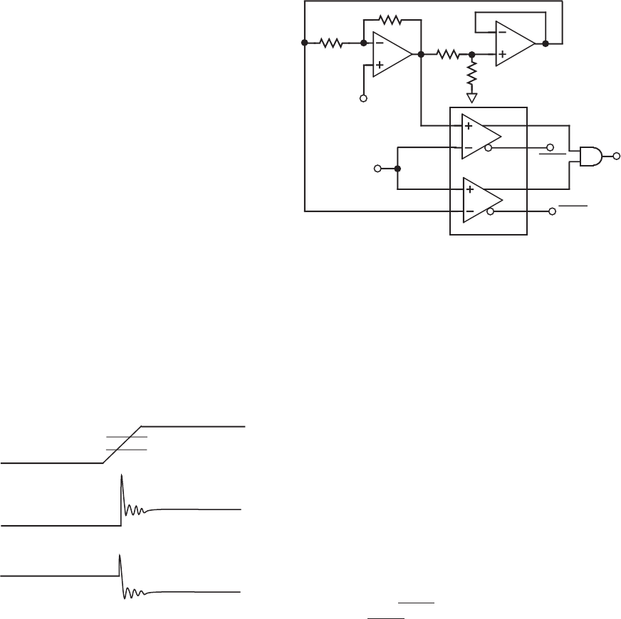
Figure 1. AD9698 Used as Window Detector
When configured as shown, the op amps generate reference lev-
els for the comparators that are equally spaced above and below
the applied V
IN
. The width of the window is established by the
ratio of R1 and R2. For a given ratio of R1 and R2, +V
REF
and
–V
REF
will be fixed percentages above and below V
IN
. As an ex-
ample, using 2.2 k for R1 and 10 k for R2 creates a ±10%
window. When V
IN
equals +3 V, +V
REF
will be +3.3 V and
–V
REF
will be +2.7 V. Likewise, for a –2 V input, the thresholds
will be –1.8 V and –2.2 V. Windows of differing percentage
width can be calculated with the equation:
(1–X)/2X = R2/R1
where:
X = % window
Additionally, the low impedance of the op amp outputs assures
that the threshold voltages will remain constant when the input
currents change as the signal passes through the threshold volt-
age levels.
The output of the AND gate will be high while the signal is in-
side the window. Q1
OUT
will be high when the signal is above
+V
REF
, and Q2
OUT
will be high when the signal is below –V
REF
.
Crystal Oscillator
Oscillators are used in a wide variety of applications from audio
circuits to waveform generators, from ATE triggers and tele-
communications transceivers to radar. Figure 2 shows a versatile
and inexpensive oscillator. The circuit uses the AD9696, in a
positive feedback mode, and is capable of generating accurate
and stable oscillations with frequencies ranging from 1 MHz to
more than 40 MHz.
To generate oscillations from 1 to 25 MHz, a fundamental
mode crystal is used without the dc blocking capacitor and
choke. The parallel capacitor on the inverting input is selected
for stability (0.1 µF for 1–10 MHz; 220 pF for frequencies
above 10 MHz).
APPLICATIONS
General
Two characteristics of the AD9696 and AD9698 should be con-
sidered for any application. First is the fact that all TTL com-
parators are prone to oscillate if the inputs are close to equal for
any appreciable period of time. One instance of this happening
would be slow changes in the unknown signal; the probability of
oscillation is reduced when the unknown signal passes through
the threshold at a high slew rate. Another instance is if the un-
known signal does not overdrive the comparator logic. Unless
they are overdriven, TTL comparators have undershoot when
switching logic states. The smaller the overdrive, the greater the
undershoot; when small enough, the comparator will oscillate,
not being able to determine a valid logic state. For the AD9696
and AD9698, 20 mV is the smallest overdrive which will assure
crisp switching of logic states without significant undershoot.
The second characteristic to keep in mind when designing
threshold circuits for these comparators is twofold: (1) bias cur-
rents change when the threshold is exceeded; and (2) ac input
impedance decreases when the comparator is in its linear region.
During the time both transistors in the differential pair are con-
ducting, the ac input impedance drops by orders of magnitude.
Additionally, the input bias current switches from one input to
the other, depending upon whether or not the threshold is ex-
ceeded. As a result, the input currents follow approximately the
characteristic curves shown below.
{
SIGNAL
VOLTAGE
AT +INPUT
+INPUT
CURRENT
– INPUT
CURRENT
LINEAR
REGION
Threshold Input Currents
This characteristic will not cause problems unless a high imped-
ance threshold circuit or drive circuit is employed. A circuit
similar to that shown in the window comparator application can
eliminate this possible problem.
Window Comparator
Many applications require determining when a signal’s voltage
falls within, above, or below a particular voltage range. A simple
tracking window comparator can provide this data. Figure 1
shows such a window comparator featuring high speed, TTL
compatibility, and ease of implementation.
Two comparators are required to establish a “window” with up-
per and lower threshold voltages. The circuit shown uses the
AD9698 dual ultrafast TTL comparator. In addition to the cost
and space savings over a design using two single comparators,
the dual comparator on a single die produces better matching of
both dc and dynamic characteristics.
PREVIOUS123NEXT