Closed Dec 25th-26th
800-300-1968
We Stock Hard to Find Parts
My Account
|
My Orders
|
My Cart
Questions?
(800) 300-1968
Register
(current)
My Account
(current)
My Orders
(current)
My Cart
(current)
Categories
(current)
Manufacturers
Request a Quote
Sell Your Excess
Consignment
Quality Assurance
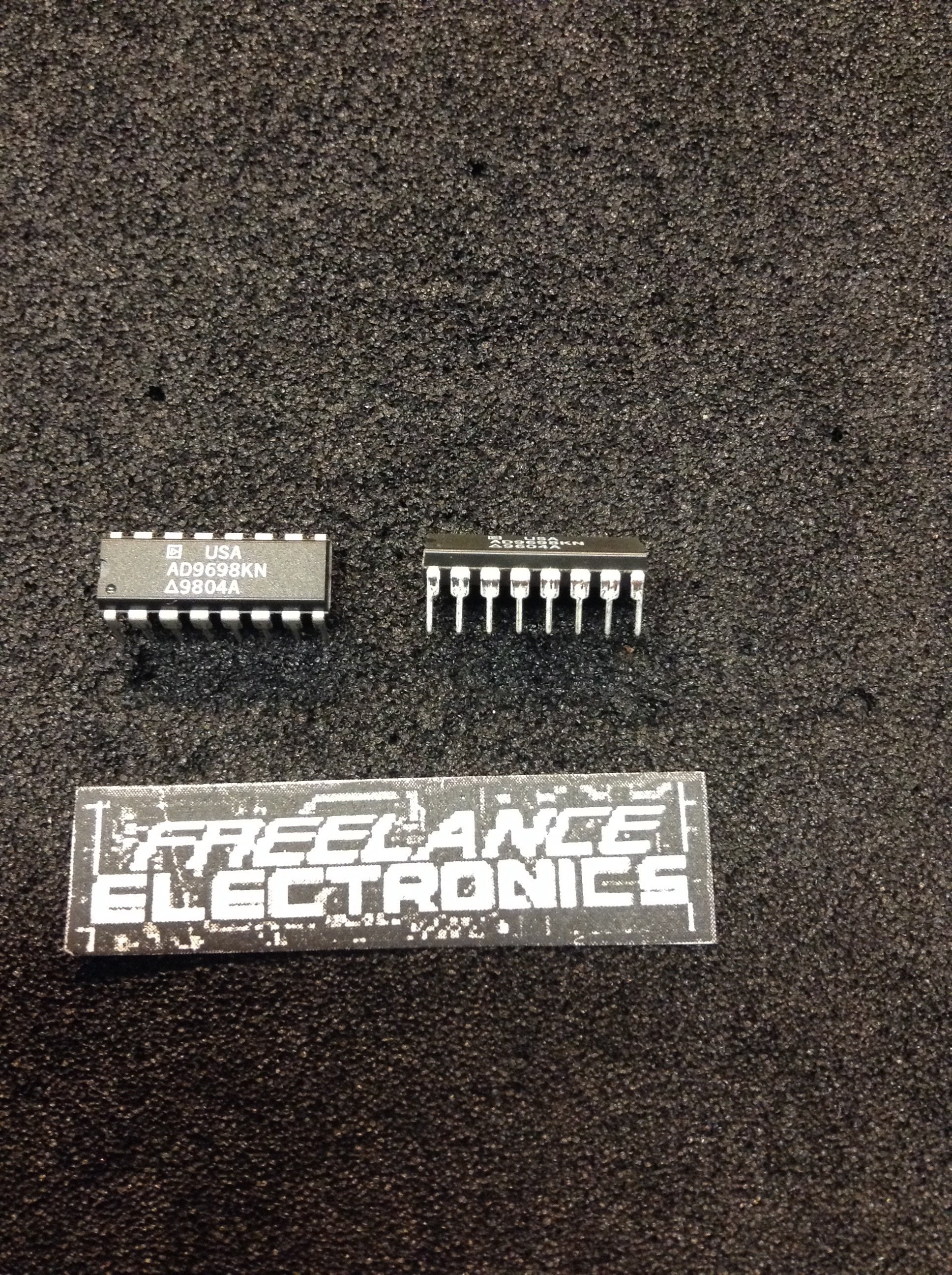
AD9698KN
Part #
AD9698KN
Description
Category
IC
Availability
In Stock
Qty
39
Qty
Price
1 - 8
$32.14432
9 - 16
$25.56935
17 - 24
$24.10824
25 - 32
$22.40362
33 +
$19.96844
Manufacturer
Available
Qty
Analog Devices
Date Code: 9600
Freelance Stock:
30
Ships Immediately
Analog Devices
Date Code: 9604
Freelance Stock:
9
Ships Immediately
Add to Cart
Related Items
Analog Devices
IC
AD9696KR
$5.21822
Analog Devices
IC
AD9696TZ/883B
$675.03054
Fairchild Semiconductor
IC
008-25424
$11.58351
Harris Corporation
IC
01-6945-9
Motorola Corp
IC
010-143121-0002
Texas Instruments
IC
01295-672141D