Closed Dec 25th-26th
800-300-1968
We Stock Hard to Find Parts
My Account
|
My Orders
|
My Cart
Questions?
(800) 300-1968
Register
(current)
My Account
(current)
My Orders
(current)
My Cart
(current)
Categories
(current)
Manufacturers
Request a Quote
Sell Your Excess
Consignment
Quality Assurance
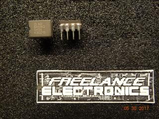
AD845KN
Part #
AD845KN
Description
OP Amp Single GP ±18V 8-Pin PDIP
Category
IC
Availability
In Stock
Qty
2
Qty
Price
1 +
$5.79280
Manufacturer
Available
Qty
Analog Devices
Date Code: 0111
Freelance Stock:
2
Ships Immediately
Add to Cart
Related Items
Analog Devices
IC
AD845AQ
$18.58939
Analog Devices
IC
AD845JN
$8.92005
Analog Devices
IC
AD845SQ/883B
$47.84540
Fairchild Semiconductor
IC
008-25424
$11.58351
Harris Corporation
IC
01-6945-9
Motorola Corp
IC
010-143121-0002