REV. 0
AD8353
–11–
THEORY OF OPERATION
The AD8353 is a two-stage feedback amplifier employing both
shunt-series and shunt-shunt feedback. The first stage is degen-
erated and resistively loaded, and provides approximately 10 dB
of gain. The second stage is a PNP-NPN Darlington output
stage, which provides another 10 dB of gain. Series-shunt feed-
back from the emitter of the output transistor sets the input
impedance to 50 Ω over a broad frequency range. Shunt-shunt
feedback from the amplifier output to the input of the Darlington
stage helps to set the output impedance to 50 Ω. The amplifier
can be operated from a 3 V supply by adding a choke inductor
from the amplifier output to VPOS. Without
this choke induc-
tor, operation from a 5 V supply is also possible.
BASIC CONNECTIONS
The AD8353 RF Gain Block is a fixed-gain amplifier with
single-ended input and output ports whose impedances are
nominally equal to 50 Ω over the frequency range 100 MHz to
2.7 GHz. Consequently, it can be directly inserted into a 50 Ω
system with no impedance-matching circuitry required. The input
and output impedances are sufficiently stable versus variations
in temperature and supply voltage that no impedance matching
compensation is required. A complete set of scattering parameters
is available at the Analog Devices website (www.analog.com).
The input pin (INPT) is connected directly to the base of the
first amplifier stage, which is internally biased to approximately 1 V,
so a dc-blocking capacitor should be connected between the
source that drives the AD8353 and the input pin, INPT.
It is critical to supply very low inductance ground connections
to the ground pins (pins 1, 4, 5, and 8) as well as to the back-
side exposed paddle. This will ensure stable operation.
The AD8353 is designed to operate over a wide supply voltage
range, from 2.7 V to 5.5 V. The output of the part, VOUT, is
taken directly from the collector of the output amplifier stage.
This node is internally biased to approximately 2.2 V when the
supply voltage is 5 V. Consequently, a dc-blocking capacitor
should be connected between the output pin, VOUT, and the
load that it drives. The value of this capacitor is not critical, but
it should be 100 pF or larger.
When the supply voltage is 3 V, it is recommended that an
external RF choke be connected between the supply voltage and
the output pin, VOUT. This will increase the dc voltage applied
to the collector of the output amplifier stage, which will improve
performance of the AD8353 to be very similar to the performance
produced when 5 V is used for the supply voltage. The inductance
of the RF choke should be approximately 100 nH, and care should
be taken to ensure that the lowest series self-resonant frequency
of this choke is well above the maximum frequency of operation
for the AD8353.
The supply voltage input, VPOS, should be bypassed using a
large value capacitance (approximately 0.47 µF or larger) and a
smaller, high-frequency bypass capacitor (approximately 100 pF)
physically located close to the VPOS pin.
The recommended connections and components are shown in
the schematic of the AD8353 evaluation board.
APPLICATIONS
The AD8353 RF Gain Block may be used as a general purpose
fixed-gain amplifier in a wide variety of applications, such as a
driver for a transmitter power amplifier (Figure 1). Its excellent
reverse isolation also makes this amplifier suitable for use as a
local oscillator buffer amplifier that would drive the local oscilla-
tor port of an up or down converter mixer (Figure 2).
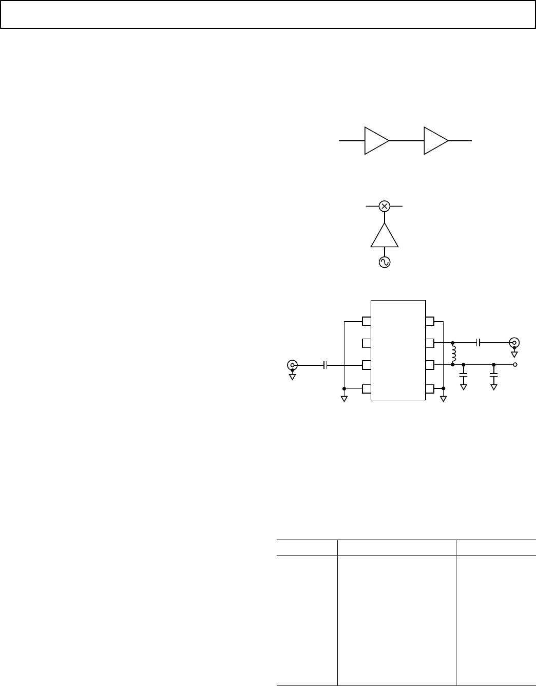
AD8353
HIGH POWER
AMPLIFIER
Figure 1. AD8353 as a Driver Amplifier
MIXER
AD8353
LOCAL
OSCILLATOR
Figure 2. AD8353 as a LO Driver Amplifier
NC = NO CONNECT
COM1
NC
INPT
COM1
VOUT
VPOS
COM2COM2
AD8353
C3
100pF
C4
0.47F
VP
OUTPUT
1
2
3
45
6
7
8
C2
1000pF
C1
1000pF
INPUT
L1
Figure 3. Evaluation Board Schematic
EVALUATION BOARD
Figure 3 shows the schematic of the AD8353 evaluation board.
Note that L1 is shown as an optional component that is used to
obtain maximum gain only when V
P
= 3 V. The board is powered
by a single supply in the range 2.7 V to 5.5 V. The power supply
is decoupled by a 0.47 µF and a 100 pF capacitor.
Table I. Evaluation Board Configuration Options
Component Function Default Value
C1, C2 AC-Coupling Capacitors 1000 pF, 0603
C3 High-Frequency Bypass
Capacitor 100 pF, 0603
C4 Low-Frequency Bypass
Capacitor 0.47 µF, 0603
L1 Optional RF Choke,
used to increase current
through
output stage
when V
P
= 3 V.
Not recommended for use
when V
P
= 5 V. 100 nH, 0603


