AD724
REV. B
–13–
The crystal should be a parallel resonant type at the appropriate
frequency (NTSC or PAL, 1FSC or 4FSC). The series combi-
nation of C1 and C2 should be approximately equal to the crys-
tal manufacturer’s specification for the parallel capacitance
required for the crystal to operate at its specified frequency. C1
will usually want to be a somewhat smaller value because of the
input parasitic capacitance of the inverter. If it is desired to tune
the frequency to greater accuracy, C1 can be made still smaller
and a parallel adjustable capacitor can be used to adjust the
frequency to the desired accuracy.
Resistor R2 serves to provide the additional phase shift
required by the circuit to sustain oscillation. It can be sized by
R2 = 1/(2 ×
π
× f × C2). Other functions of R2 are to provide a
low-pass filter that suppresses oscillations at harmonics of the
fundamental of the crystal, and to isolate the output of the in-
verter from the strange load that the crystal network presents.
The basic oscillator described above is buffered by U1B to drive
the AD724 FIN pin and other devices in the system. For a
system that requires both an NTSC and PAL oscillator, the
circuit can be duplicated by using a different pair of inverters
from the same package.
Dot Crawl
Numerous distortions are apparent in the presentation of com-
posite signals on TV monitors. These effects will vary in degree,
depending on the circuitry used by the monitor to process the
signal, and on the nature of the image being displayed. It is
generally not possible to produce pictures on a composite moni-
tor that are as high quality as those produced by standard qual-
ity RGB, VGA monitors.
One well known distortion of composite video images is called
dot crawl. It shows up as a moving dot pattern at the interface
between two areas of different color. It is caused by the inability
of the monitor circuitry to adequately separate the luminance
and chrominance signals.
One way to prevent dot crawl is to use a video signal with sepa-
rate luminance and chrominance. Such a signal is referred to as
S-video or Y/C video. Since the luminance and chrominance are
already separated, the monitor does not have to perform this
function. The S-Video outputs of the AD724 can be used to
create higher quality pictures when there is an S-Video input
available on the monitor.
Flicker
In a VGA conversion application, where the software controlled
registers are correctly set, two techniques are commonly used by
VGA controller manufacturers to generate the interlaced signal.
Each of these techniques introduces a unique characteristic into
the display created by the AD724. The artifacts described below
are not due to the encoder or its encoding algorithm as all en-
coders will generate the same display when presented with these
inputs. They are due to the method used by the controller dis-
play chip to convert a noninterlaced output to an interlaced
signal.
The first interlacing technique outputs a true interlaced signal
with odd and even fields (one each to a frame Figure 19a). This
provides the best picture quality when displaying photography,
CD video and animation (games, etc.). It will, however intro-
duce a defect, commonly referred to as flicker, into the display.
The VM700A has a special measurement mode that enables it
to directly measure the frequency of one subcarrier in a video
waveform with respect to an internally stored reference or a
simultaneously supplied reference. The instrument gives a read-
ing of the relative frequencies of the reference and test signals in
units of 0.1␣ Hz. This is not a direct reading of the subcarrier
frequency in MHz but a relative reading in Hz of the difference
in frequency between the two signals.
If the reference video source is supplied by a video generator
that has a CW subcarrier output, its CW subcarrier can be
measured with a frequency counter to accurately determine its
frequency. The AD724 circuit under test can then be measured
relative to this reference by using the built in color burst mea-
suring function of the VM700A, and the offset frequency
measured can be added to or subtracted from the measured
frequency of the CW subcarrier to determine the operating
frequency of the DUT.
It should be noted that the VM700A is a highly specialized
video measurement instrument. In order for it to synchronize
on a video signal, the synchronization pattern of the signal must
adhere very closely to the appropriate video standard. In par-
ticular, a video signal that is missing equalization and serration
pulses from the vertical blanking interval will cause the “Loss of
Sync” message to be displayed by the VM700A. Many such
signals might make a perfectly acceptable picture on a monitor,
but will not be recognized by the VM700A.
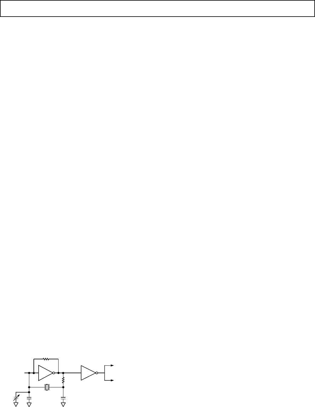
Low Cost Crystal Oscillator
If a crystal is used with the on-chip oscillator of the AD724,
there will be no CW clock available that can be used elsewhere
in the system: the only AD724 signals that output this fre-
quency are the chrome and composite that have only colorburst
and chrominance at the subcarrier frequency. These cannot be
used for clocking other devices.
A low cost oscillator can be made to provide a CW clock that
can be used to drive both the AD724 FIN and other devices in
the system that require a clock at this frequency. In addition,
the same technique can be used to make a clock signal at a
4FSC, which might be required by other devices and can also
be used to drive the FIN pin of the AD724.
Figure 18 shows a circuit that uses one inverter of a 74HC04
package to create a crystal oscillator and another inverter to
buffer the oscillator and drive other loads. The logic family
must be a CMOS type that can support the frequency of opera-
tion, and it must NOT be a Schmitt trigger type of inverter.
Resistor R1 from input to output of U1A linearizes the inverter’s
gain so it provides useful gain and a 180 degree phase shift to
drive the oscillator.
R1
1MV
Y1
TO PIN 3
OF AD724
U1A U1B
R2
1kV
C2
60pF
C1
47pF
C3
~
15pF
(OPT)
TO OTHER
DEVICE CLOCKS
HC04
HC04
Figure 18. Low Cost Crystal Oscillator


