Closed Dec 25th-26th
800-300-1968
We Stock Hard to Find Parts
My Account
|
My Orders
|
My Cart
Questions?
(800) 300-1968
Register
(current)
My Account
(current)
My Orders
(current)
My Cart
(current)
Categories
(current)
Manufacturers
Request a Quote
Sell Your Excess
Consignment
Quality Assurance
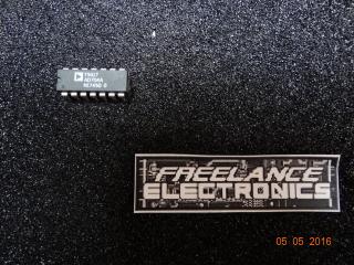
AD704KN
Part #
AD704KN
Description
IC OPAMP GP 4 CIRCUIT 14DIP
Category
IC
Availability
In Stock
Qty
1
Qty
Price
1 +
$9.81156
Manufacturer
Available
Qty
Analog Devices
Date Code: 9404
Freelance Stock:
1
Ships Immediately
Add to Cart
Related Items
Analog Devices
IC
AD704A
$13.52287
Analog Devices
IC
AD704AQ
$22.80640
Analog Devices
IC
AD704JN
$7.31722
Analog Devices
IC
AD704JR
$8.19680
Analog Devices
IC
AD704TQ
$52.52382
Fairchild Semiconductor
IC
008-25424
$11.58351