Closed Dec 25th-26th
800-300-1968
We Stock Hard to Find Parts
My Account
|
My Orders
|
My Cart
Questions?
(800) 300-1968
Register
(current)
My Account
(current)
My Orders
(current)
My Cart
(current)
Categories
(current)
Manufacturers
Request a Quote
Sell Your Excess
Consignment
Quality Assurance
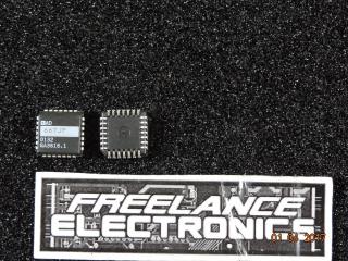
AD667AD
Part #
AD667AD
Description
DAC 1CH CURRENT STEERING 12-BIT 28PIN SBCDIP - Rail/Tube
Category
IC
Availability
Out of Stock
Qty
0
Qty
Price
1 +
$17.32466
Related Items
Analog Devices
IC
AD667BD
$35.80632
Analog Devices
IC
AD667JP
$21.69357
Analog Devices
IC
AD667KN
$27.85435
Analog Devices
IC
AD667KN/+
$18.87261
Analog Devices
IC
AD667SD
$124.54727
Analog Devices
IC
AD667SE
$213.15343