Closed Dec 25th-26th
800-300-1968
We Stock Hard to Find Parts
My Account
|
My Orders
|
My Cart
Questions?
(800) 300-1968
Register
(current)
My Account
(current)
My Orders
(current)
My Cart
(current)
Categories
(current)
Manufacturers
Request a Quote
Sell Your Excess
Consignment
Quality Assurance
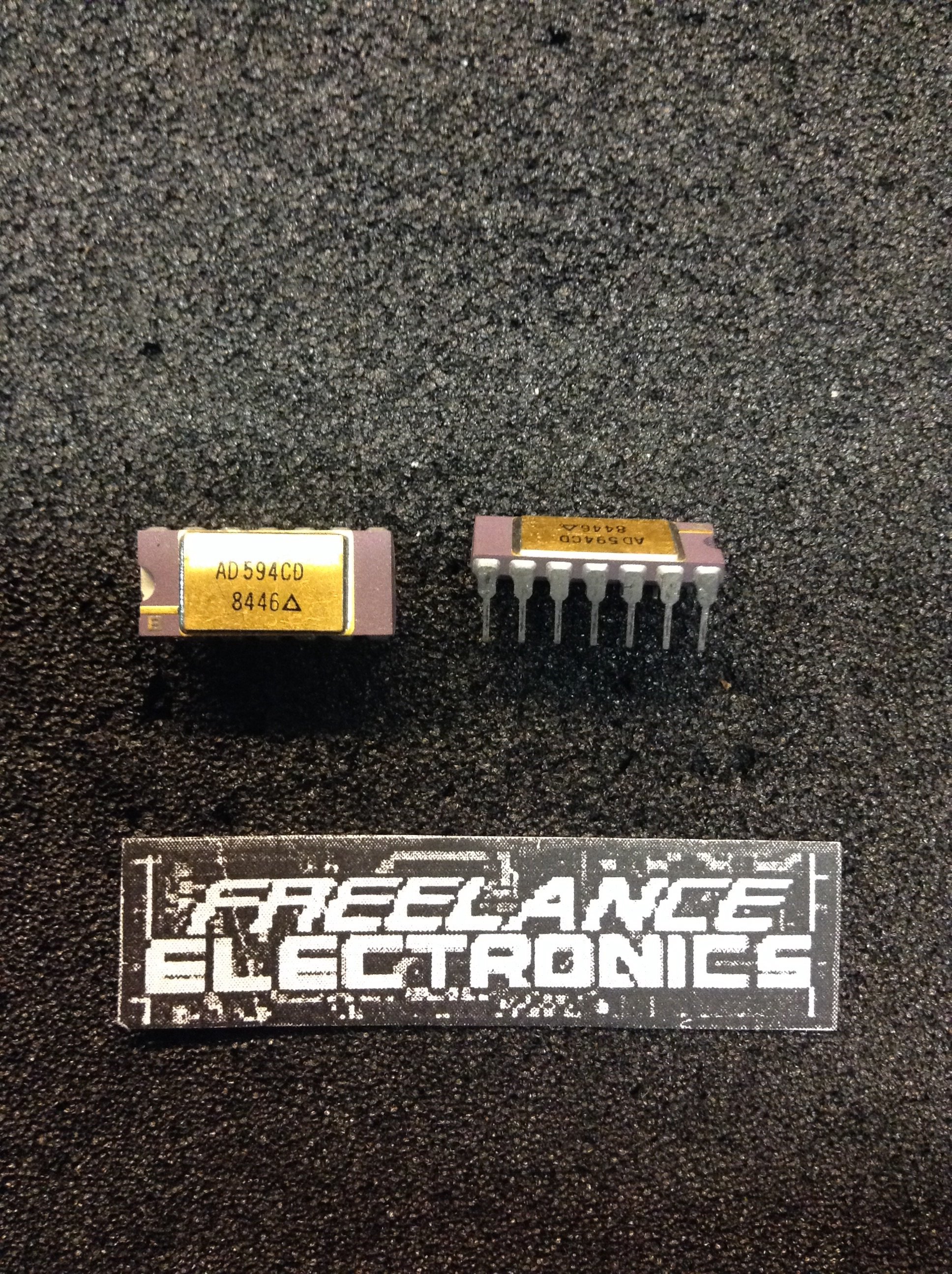
AD594CD
Part #
AD594CD
Description
Temp Sensor Analog 14-Pin TO-116 Tube
Category
IC
Availability
In Stock
Qty
50
Qty
Price
1 - 3
$47.54785
4 - 7
$37.82216
8 - 15
$35.66089
16 - 23
$33.13941
24 +
$29.53730
Manufacturer
Available
Qty
Analog Devices
Date Code: 8446
Freelance Stock:
50
Ships Immediately
Add to Cart
Related Items
Analog Devices
IC
AD594AD
$16.86837
Fairchild Semiconductor
IC
008-25424
$11.58351
Harris Corporation
IC
01-6945-9
Motorola Corp
IC
010-143121-0002
Texas Instruments
IC
01295-672141D
Military Spec
IC
01405915