Closed Dec 25th-26th
800-300-1968
We Stock Hard to Find Parts
My Account
|
My Orders
|
My Cart
Questions?
(800) 300-1968
Register
(current)
My Account
(current)
My Orders
(current)
My Cart
(current)
Categories
(current)
Manufacturers
Request a Quote
Sell Your Excess
Consignment
Quality Assurance
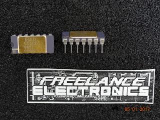
AD534LH
Part #
AD534LH
Description
ANALOG MULTIPLIER, 20V/uS, TO-100-10, No. of Multipliers /
Category
IC
Availability
Out of Stock
Qty
0
Qty
Price
1 +
$64.53000
Related Items
Analog Devices
IC
AD5341BRU
$6.47001
Analog Devices
IC
AD5344BRU
$17.36436
Analog Devices
IC
AD534JD
$24.40811
Analog Devices
IC
AD534KD
$105.53004
Analog Devices
IC
AD534SD
$100.68512
Analog Devices
IC
AD534TE/883B-Q
$100.00000