Freelance Electronics Components Distributor
Closed Dec 25th-26th
800-300-1968
We Stock Hard to Find Parts

AD2S83AP

Part # AD2S83AP
Description RESOLVER TO DGTL CNVRTR 44PLCC - Rail/Tube
Category IC
Availability Out of Stock
Qty 0
Qty Price
1 + $108.42360


Technical Document


DISCLAIMER: The information provided herein is solely for informational purposes. Customers must be aware of the suitability of this product for their application, and consider that variable factors such as Manufacturer, Product Category, Date Codes, Pictures and Descriptions may differ from available inventory.

AD2S83–SPECIFICATIONS
AD2S83
Parameter Conditions Min Typ Max Units
THREE-STATE LEAKAGE DB1–DB16 Only
Current I
L
±V
S
= ±12.0 V, V
L
= 5.5 V
20 µA
V
OL
= 0 V
±V
S
= ±12.0 V, V
L
= 5.5 V
20 µA
V
OH
= 5.0 V
RATIO MULTIPLIER
AC Error Output Scaling 10 Bit 177.6 mV/Bit
12 Bit 44.4 mV/Bit
14 Bit 11.1 mV/Bit
16 Bit 2.775 mV/Bit
PHASE SENSITIVE DETECTOR
Output Offset Voltage 12 mV
Gain
In Phase w.r.t. REF –0.882 –0.9 –0.918 V rms/V dc
In Quadrature w.r.t. REF ±0.02 V rms/V dc
Input Bias Current 60 150 nA
Input Impedance 1.0 M
Input Voltage ±8V
INTEGRATOR
Open-Loop Gain At 10 kHz 57 60 63 dB
Dead Zone Current (Hysteresis) 90 100 110 nA/LSB
Input Offset Voltage 15 mV
Input Bias Current 60 150 nA
Output Voltage Range 8 V
VCO
Maximum Rate 1.1 MHz
VCO Rate +ve DIR 8.25 8.50 8.75 kHz/µA
–ve DIR 8.25 8.50 8.75 kHz/µA
VCO Power Supply Sensitivity
Rate +V
S
+0.5 %/V
–V
S
–0.5 %/V
Input Offset Voltage 3mV
Input Bias Current 12 50 nA
Input Bias Current Tempco +0.22 nA/°C
Linearity of Absolute Rate
AD2S83AP
0 kHz–500 kHz ±0.15 0.25 % FSR
0.5 MHz–1 MHz ±0.25 1.0 % FSR
AD2S83IP
0 kHz–500 kHz ±0.25 0.5 % FSR
0.5 MHz–1 MHz ±0.25 1.0 % FSR
Reversion Error
AD2S83AP ±0.5 1.0 % Output
AD2S83IP ±1.0 1.5 % Output
POWER SUPPLIES
Voltage Levels
+V
S
+11.4 +12.6 V
–V
S
–11.4 –12.6 V
+V
L
+4.5 +5 +V
S
V
Current
±I
S
±V
S
@ ± 12 V ±12 23 mA
±I
S
±V
S
@ ±12.6 V ±19 30 mA
±I
L
+V
L
@ ±5.0 V ±0.5 1.5 mA
All min and max specifications are guaranteed. Specifications in boldface are tested on all production units at final electrical test.
Specification subject to change without notice.
(V
S
= 12 V dc 5%; V
L
= +5 V dc 10%; T
A
= –40C to +85C)
ORDERING GUIDE
Temperature Package Package
Model Range Accuracy Description Option
AD2S83AP –40°C to +85°C 8 arc min Plastic Leaded Chip Carrier P-44A
AD2S83IP –40°C to +85°C 8 arc min Plastic Leaded Chip Carrier P-44A
REV. D
–4–
AD2S83
–5–
REV. D
PIN FUNCTION DESCRIPTIONS
P
in
Nos. Mnemonic Description
1 DEMOD O/P Demodulator Output
2 REFERENCE I/P Reference Signal Input
3 AC ERROR O/P Ratio Multiplier Output
4 COS Cosine Input
5 ANALOG GND Power Ground
6 SIGNAL GND Resolver Signal Ground
7 SIN Sine Input
8+V
S
Positive Power Supply
10–25 DB1–DB16 Parallel Output Data
26 +V
L
Logic Power Supply
27 ENABLE Logic HI—Output Data Pins in
High Impedance State
Logic LO—Presents Active Data
to the Output Pins
28 BYTE SELECT Logic HI—Most Significant Byte to
DB1–DB8
Logic LO—Least Significant Byte
to DB1–DB8
30 INHIBIT Logic LO Inhibits Data Transfer
to Output Latches
31 DIGITAL GND Digital Ground
32, 33 SC2–SC1 Select Converter Resolution
34 DATA LOAD Logic LO DB1–DB16 Inputs
Logic HI DB1–DB16 Outputs
35 COMPLEMENT Active Logic LO
36 BUSY Converter Busy, Data not Valid
While Busy HI
37 DIRECTION Logic State Defines Direction of
Input Signal Rotation
38 RIPPLE CLOCK Positive Pulse When Converter Output
Changes from 1s to All 0s or Vice Versa
39 –V
S
Negative Power Supply
40 VCO I/P VCO Input
41 VCO O/P VCO Output
42 INTEGRATOR O/P Integrator Output
43 INTEGRATOR I/P Integrator Input
44 DEMOD I/P Demodulator Input
ABSOLUTE MAXIMUM RATINGS
1
(with respect to GND)
+V
S
2
. . . . . . . . . . . . . . . . . . . . . . . . . . . . . . . . . . . . . +13 V dc
–V
S
2
. . . . . . . . . . . . . . . . . . . . . . . . . . . . . . . . . . . . . –13 V dc
+V
L
. . . . . . . . . . . . . . . . . . . . . . . . . . . . . . . . . . . . . . . . . . +V
S
Reference . . . . . . . . . . . . . . . . . . . . . . . . . . . . . . . +13 V to –V
S
SIN . . . . . . . . . . . . . . . . . . . . . . . . . . . . . . . . . . . +13 V to –V
S
COS . . . . . . . . . . . . . . . . . . . . . . . . . . . . . . . . . . +13 V to –V
S
Any Logical Input . . . . . . . . . . . . . . . . . . –0.4 V dc to +V
L
dc
Demodulator Input . . . . . . . . . . . . . . . . . . . . . . . +13 V to –V
S
Integrator Input . . . . . . . . . . . . . . . . . . . . . . . . . . +13 V to –V
S
VCO Input . . . . . . . . . . . . . . . . . . . . . . . . . . . . . +13 V to –V
S
Power Dissipation . . . . . . . . . . . . . . . . . . . . . . . . . . . 800 mW
Operating Temperature
Industrial (AP, IP) . . . . . . . . . . . . . . . . . . . –40°C to +85°C
Storage Temperature . . . . . . . . . . . . . . . . . . –65°C to +150°C
Lead Temperature (Soldering, 10 sec) . . . . . . . . . . . . +300°C
CAUTION
1
Absolute Maximum Ratings are those values beyond which damage to the device
may occur.
2
Correct polarity voltages must be maintained on the +V
S
and –V
S
pins.
RECOMMENDED OPERATING CONDITIONS
Power Supply Voltage (+V
S
, –V
S
) . . . . . . . . . . ±12 V dc ± 5%
Power Supply Voltage V
L
. . . . . . . . . . . . . . . . . +5 V dc ± 10%
Analog Input Voltage (SIN and COS) . . . . . . . .2 V rms ± 10%
Analog Input Voltage (REF) . . . . . . . . . . . . . . 1 V to 8 V peak
Signal and Reference Harmonic Distortion . . . . . . . 10% (max)
Phase Shift Between Signal and Reference . . . ±10 Degrees (max)
Ambient Operating Temperature Range
Industrial (AP, IP) . . . . . . . . . . . . . . . . . . . . –40°C to +85°C
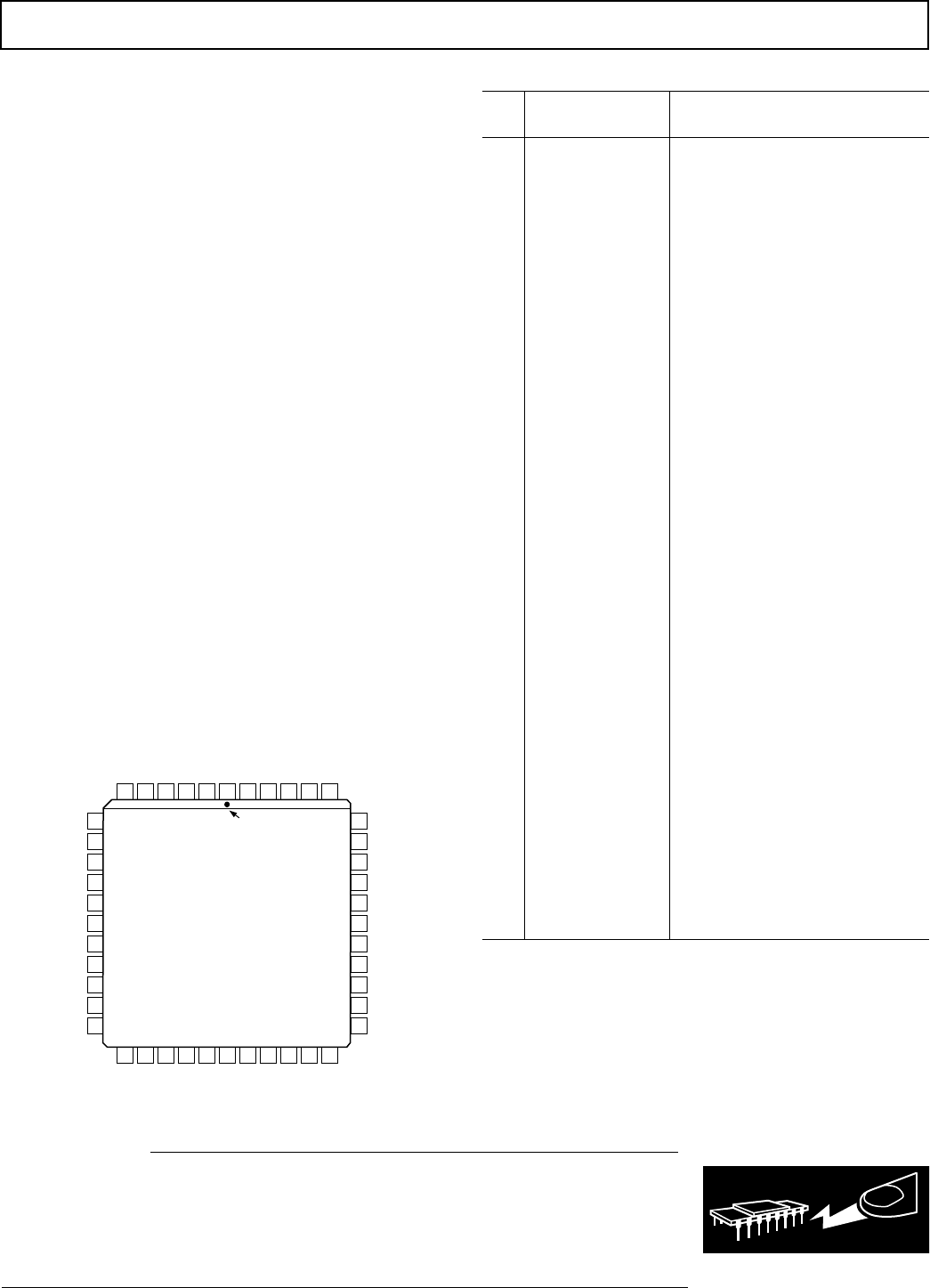
PIN CONFIGURATION
9
10
11
12
13
7
8
16
17
14
15
21443
4
5642414043
35
36
37
38
39
33
34
31
32
29
30
–V
S
RIPPLE CLOCK
DIRECTION
BUSY
COMP
DATA LOAD
SC1
DB14
DB11
DB12
DB13
DB15
SIN I/P
+V
S
NC
(MSB) DB1
DB2
DB3
DB4
NC = NO CONNECT
DB5
DB6
DB7
DB8
SC2
DIGITAL GND
INHIBIT
NC
SIGNAL GND
ANALOG GND
COS I/P
AC ERROR O/P
REF I/P
DEMOD O/P
DEMOD I/P
INTEGRATOR I/P
INTEGRATOR O/P
VCO O/P
VCO I/P
18
19
20 21 22 23 24 25
26
27 28
PIN 1
IDENTIFIER
TOP VIEW
(Not to Scale)
AD2S83
(LSB) DB16
+V
L
ENABLE
BYTE SELECT
DB10
DB9
ESD SENSITIVITY
The AD2S83 features an input protection circuit consisting of large “distributed” diodes and
polysilicon series resistors to dissipate both high energy discharge (Human Body Model) and fast, low
energy pulses (Charges Device Model).
Proper ESD protection are strongly recommended to avoid functional damage or performance
degradation. For further information on ESD precautions, refer to Analog Devices ESD Prevention
Manual.
WARNING!
ESD SENSITIVE DEVICE
AD2S83
REV. D
–6–
Bit Weight Table
Binary Resolution Degrees Minutes Seconds
Bits (N) (N
N
) /Bit /Bit /Bit
0 1 360.0 21600.0 1296000.0
1 2 180.0 10800.0 648000.0
2 4 90.0 5400.0 324000.0
3 8 45.0 2700.0 162000.0
4 16 22.5 1350.0 81000.0
5 32 11.25 675.0 40500.0
6 64 5.625 337.5 20250.0
7 128 2.8125 168.75 10125.0
8 256 1.40625 84.375 5062.5
9 512 0.703125 42.1875 2531.25
10 1024 0.3515625 21.09375 1265.625
11 2048 0.1757813 10.546875 632.8125
12 4096 0.0878906 5.273438 316.40625
13 8192 0.0439453 2.636719 158.20313
14 16384 0.0219727 1.318359 79.10156
15 32768 0.0109836 0.659180 39.55078
16 65536 0.0054932 0.329590 19.77539
17 131072 0.0027466 0.164795 9.88770
18 262144 0.0013733 0.082397 4.94385
CONNECTING THE CONVERTER
The power supply voltages connected to +V
S
and –V
S
pins
should be +12 V dc and –12 V dc and must not be reversed.
The voltage applied to V
L
can be +5 V dc to +V
S
.
It is recommended that the decoupling capacitors are connected
in parallel between the power lines +V
S
, –V
S
and ANALOG
GROUND adjacent to the converter. Recommended values are
100 nF (ceramic) and 10 µF (tantalum). Also capacitors of
100 nF and 10 µF should be connected between +V
L
and
DIGITAL GROUND adjacent to the converter.
When more than one converter is used on a card, separate de-
coupling capacitors should be used for each converter.
The resolver connections should be made to the SIN and COS
inputs, REFERENCE INPUT and SIGNAL GROUND as
shown in Figure 11 and described in the Connecting the
Resolver section.
The two signal ground wires from the resolver should be joined
at the SIGNAL GROUND pin of the converter to minimize the
coupling between the sine and cosine signals. For this reason it
is also recommended that the resolver is connected using indi-
vidually screened twisted pair cables with the sine, cosine and
reference signals twisted separately.
SIGNAL GROUND and ANALOG GROUND are connected
internally. ANALOG GROUND and DIGITAL GROUND
must be connected externally and as close to the converter as
possible.
The external components required should be connected as
shown in Figure 1.
CONVERTER RESOLUTION
Two major areas of the AD2S83 specification can be selected by
the user to optimize the total system performance. The resolu-
tion of the digital output is set by the logic state of the inputs
SC1 and SC2 to be 10, 12, 14 or 16 bits; and the dynamic char-
acteristics of bandwidth and tracking rate are selected by the
choice of external components.
The choice of the resolution will affect the values of R4 and R6
which scale the inputs to the integrator and the VCO respec-
tively (see Component Selection section). If the resolution is
changed, then new values of R4 and R6 must be switched into
the circuit.
Note: When changing resolution under dynamic conditions, do
it when the BUSY is low, i.e., when data is not changing.
A1
A2
SEGMENT
SWITCHING
RIPPLE
CLOCK
TRACKING
RATE
SELECTION
VELOCITY
SIGNAL
R5
C4
C5
INTEGRATOR
I/P
BANDWIDTH
SELECTION
R8
–12V
+12V
OFFSET ADJUST
R9
R3
C3
REFERENCE
I/P
HF FILTER
R2
C2
C1
R1
DEMOD
O/P
PHASE
SENSITIVE
DETECTOR
INTEGRATOR
O/P
DIRECTIONBUSYDIG
GND
16 DATA BITS
SC1
SC2
DATA
LOAD
BYTE
SELECT
+5V
+12V
–12V
GND
COS
SIG GND
SIN
AC ERROR O/P
AD2S83
VCO
O/P
VCO
I/P
C7
150pF
VCO + DATA
TRANSFER
LOGIC
A3
R4
R7
3K3
C6
390pF
OUTPUT DATA LATCH
R - 2R DAC
16-BIT UP/DOWN COUNTER
R6
INHIBIT
ENABLE
Figure 1. Connection Diagram
PREVIOUS1234567NEXT