Freelance Electronics Components Distributor
Closed Dec 25th-26th
800-300-1968
We Stock Hard to Find Parts

AD1674AD

Part # AD1674AD
Description
Category IC
Availability Out of Stock
Qty 0
Qty Price
1 + $33.54250


Technical Document


DISCLAIMER: The information provided herein is solely for informational purposes. Customers must be aware of the suitability of this product for their application, and consider that variable factors such as Manufacturer, Product Category, Date Codes, Pictures and Descriptions may differ from available inventory.

AD1674–SPECIFICATIONS
AC SPECIFICATIONS
AD1674J/A AD1674K/B/T
Parameter Min Typ Max Min Typ Max Units
Signal to Noise and Distortion (S/N+D) Ratio
2, 3
69 70 70 71 dB
Total Harmonic Distortion (THD)
4
–90 –82 –90 –82 dB
0.008 0.008 %
Peak Spurious or Peak Harmonic Component –92 –82 –92 –82 dB
Full Power Bandwidth 1 1 MHz
Full Linear Bandwidth 500 500 kHz
Intermodulation Distortion (IMD)
5
Second Order Products –90 –80 –90 –80 dB
Third Order Products –90 –80 –90 –80 dB
SHA (Specifications are Included in Overall Timing Specifications)
Aperture Delay 50 50 ns
Aperture Jitter 250 250 ps
Acquisition Time 1 1 µs
DIGITAL SPECIFICATIONS
Parameter Test Conditions Min Max Units
LOGIC INPUTS
V
IH
High Level Input Voltage +2.0 V
LOGIC
+0.5 V V
V
IL
Low Level Input Voltage –0.5 +0.8 V
I
IH
High Level Input Current (V
IN
= 5 V) V
IN
= V
LOGIC
–10 +10 µA
I
IL
Low Level Input Current (V
IN
= 0 V) V
IN
= 0 V –10 +10 µA
C
IN
Input Capacitance 10 pF
LOGIC OUTPUTS
V
OH
High Level Output Voltage I
OH
= 0.5 mA +2.4 V
V
OL
Low Level Output Voltage I
OL
= 1.6 mA +0.4 V
I
OZ
High-Z Leakage Current V
IN
= 0 to V
LOGIC
–10 +10 µA
C
OZ
High-Z Output Capacitance 10 pF
NOTES
1
f
IN
amplitude = –0.5 dB (9.44 V p-p) 10 V bipolar mode unless otherwise noted. All measurements referred to –0 dB (9.997 V p-p) input signal unless
otherwise noted.
2
Specified at worst case temperatures and supplies after one minute warm-up.
3
See Figures 12 and 13 for other input frequencies and amplitudes.
4
See Figure 11.
5
fa = 9.08 kHz, fb = 9.58 kHz with f
SAMPLE
= 100 kHz. See Definition of Specifications section and Figure 15.
All min and max specifications are guaranteed.
Specifications subject to change without notice.
–4–
REV. C
(T
MIN
to T
MAX
, with V
CC
= +15 V 6 10% or +12 V 6 5%, V
LOGIC
= +5 V 6 10%, V
EE
= –15 V 610% or
–12 V 6 5%, f
SAMPLE
= 100 kSPS, f
IN
= 10 kHz, stand-alone mode unless otherwise noted)
1
(for all grades T
MIN
to T
MAX
, with V
CC
= +15 V 6 10% or +12 V 6 5%, V
LOGIC
= +5 V 6 10%,
V
EE
= –15 V 6 10% or –12 V 6 5%)
AD1674
REV. C
–5–
(for all grades T
MIN
to T
MAX
with V
CC
= +15 V 6 10% or +12 V 6 5%,
V
LOGIC
= +5 V 610%, V
EE
= –15 V 6 10% or –12 V 6 5%; V
IL
= 0.4 V,
V
IH
= 2.4 V unless otherwise noted)
SWITCHING SPECIFICATIONS
CONVERTER START TIMING (Figure 1)
J, K, A, B, Grades T Grade
Parameter Symbol Min Typ Max Min Typ Max Units
Conversion Time
8-Bit Cycle t
C
78 78µs
12-Bit Cycle t
C
910 910µs
STS Delay from CE t
DSC
200 225 ns
CE Pulse Width t
HEC
50 50 ns
CS to CE Setup t
SSC
50 50 ns
CS Low During CE High t
HSC
50 50 ns
R/C to CE Setup t
SRC
50 50 ns
R/C Low During CE High t
HRC
50 50 ns
A
0
to CE Setup t
SAC
00ns
A
0
Valid During CE High t
HAC
50 50 ns
READ TIMING—FULL CONTROL MODE (Figure 2)
J, K, A, B, Grades T Grade
Parameter Symbol Min Typ Max Min Typ Max Units
Access Time t
DD
1
75 150 75 150 ns
Data Valid After CE Low t
HD
25
2
25
2
ns
20
3
15
4
ns
Output Float Delay t
HL
5
150 150 ns
CS to CE Setup t
SSR
50 50 ns
R/C to CE Setup t
SRR
00ns
A
0
to CE Setup t
SAR
50 50 ns
CS Valid After CE Low t
HSR
00ns
R/C High After CE Low t
HRR
00ns
A
0
Valid After CE Low t
HAR
50 50 ns
NOTES
1
t
DD
is measured with the load circuit of Figure 3 and is defined as the time
required for an output to cross 0.4 V or 2.4 V.
2
0°C to T
MAX
.
3
At –40°C.
4
At –55°C.
5
t
HL
is defined as the time required for the data lines to change 0.5 V when
loaded with the circuit of Figure 3.
All min and max specifications are guaranteed.
Specifications subject to change without notice.
Test V
CP
C
OUT
Access Time High Z to Logic Low 5 V 100 pF
Float Time Logic High to High Z 0 V 10 pF
Access Time High Z to Logic High 0 V 100 pF
Float Time Logic Low to High Z 5 V 10 pF
t
HEC
CE
STS
DB11 – DB0
A
0
CS
__
R/C
_
t
SSC
t
HSC
t
SRC
t
HRC
t
SAC
t
HAC
t
C
t
DSC
HIGH IMPEDANCE
Figure 1. Converter Start Timing
HIGH
IMPEDANCE
CE
STS
DB11 – DB0
A
0
CS
__
R/C
_
t
HSR
t
SSR
t
HRR
t
SAR
t
HAR
t
DD
t
HL
HIGH
IMP.
DATA
VALID
t
HD
t
HS
t
SSR
Figure 2. Read Timing
V
CP
D
OUT
C
OUT
I
OH
I
OL
Figure 3. Load Circuit for Bus Timing Specifications
AD1674
REV. C
–6–
ORDERING GUIDE
INL S/(N+D) Package Package
Model
1
Temperature Range (T
MIN
to T
MAX
)(T
MIN
to T
MAX
) Description Option
2
AD1674JN 0°C to +70°C ±1 LSB 69 dB Plastic DIP N-28
AD1674KN 0°C to +70°C ± 1/2 LSB 70 dB Plastic DIP N-28
AD1674JR 0°C to +70°C ±1 LSB 69 dB Plastic SOIC R-28
AD1674KR 0°C to +70°C ±1/2 LSB 70 dB Plastic SOIC R-28
AD1674AR –40°C to +85°C ± 1 LSB 69 dB Plastic SOIC R-28
AD1674BR –40°C to +85°C ± 1/2 LSB 70 dB Plastic SOIC R-28
AD1674AD –40°C to +85°C ±1 LSB 69 dB Ceramic DIP D-28
AD1674BD –40°C to +85°C ± 1/2 LSB 70 dB Ceramic DIP D-28
AD1674TD –55°C to +125°C ± 1 LSB 70 dB Ceramic DIP D-28
NOTES
1
For details on grade and package offerings screened in accordance with MIL-STD-883, refer to the Analog Devices Military Products Databook or current
AD1674/883B data sheet. SMD is also available.
2
N = Plastic DIP; D = Hermetic Ceramic DIP; R = Plastic SOIC.
TIMING—STAND-ALONE MODE (Figures 4a and 4b)
J, K, A, B Grades T Grade
Parameter Symbol Min Typ Max Min Typ Max Units
Data Access Time t
DDR
150 150 ns
Low R/
C Pulse Width t
HRL
50 50 ns
STS Delay from R/
C t
DS
200 225 ns
Data Valid After R/
C Low t
HDR
25 25 ns
STS Delay After Data Valid t
HS
0.6 0.8 1.2 0.6 0.8 1.2 µs
High R/C Pulse Width t
HRH
150 150 ns
NOTE
All min and max specifications are guaranteed.
Specifications subject to change without notice.
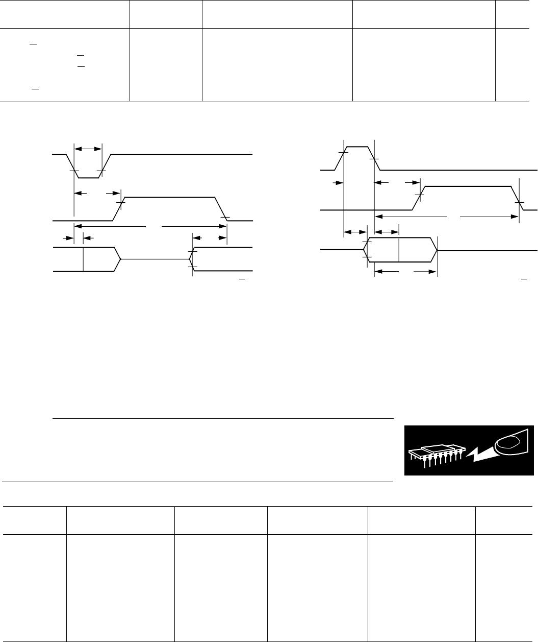
WARNING!
ESD SENSITIVE DEVICE
CAUTION
ESD (electrostatic discharge) sensitive device. Electrostatic charges as high as 4000 V readily
accumulate on the human body and test equipment and can discharge without detection. Although
the AD1674 features proprietary ESD protection circuitry, permanent damage may occur on
devices subjected to high energy electrostatic discharges. Therefore, proper ESD precautions are
recommended to avoid performance degradation or loss of functionality.
DATA
VALID
DATA VALID
HIGH-Z
STS
DB11 – DB0
R/C
_
t
HRL
t
DS
t
C
t
HS
t
HDR
Figure 4a. Stand-Alone Mode Timing Low Pulse for R/
C
DATA
VALID
HIGH-Z
HIGH-Z
STS
DB11 – DB0
R/C
_
t
HRH
t
DS
t
C
t
DDR
t
HDR
t
HL
Figure 4b. Stand-Alone Mode Timing High Pulse for R/
C
ABSOLUTE MAXIMUM RATINGS*
V
CC
to Digital Common . . . . . . . . . . . . . . . . . . . 0 to + 16.5 V
V
EE
to Digital Common . . . . . . . . . . . . . . . . . . . . . 0 to –16.5 V
V
LOGIC
to Digital Common . . . . . . . . . . . . . . . . . . 0 V to +7 V
Analog Common to Digital Common . . . . . . . . . . . . . . . ±1 V
Digital Inputs to Digital Common . . . –0.5 V to V
LOGIC
+0.5 V
Analog Inputs to Analog Common . . . . . . . . . . . . V
EE
to V
CC
20 V
IN
to Analog Common . . . . . . . . . . . . . . . . . V
EE
to +24 V
REF OUT . . . . . . . . . . . . . . . . . Indefinite Short to Common
. . . . . . . . . . . . . . . . . . . . . . . . . . . Momentary Short to V
CC
Junction Temperature . . . . . . . . . . . . . . . . . . . . . . . . . +175°C
Power Dissipation . . . . . . . . . . . . . . . . . . . . . . . . . . . .825 mW
Lead Temperature, Soldering (10 sec) . . . . . . . +300°C, 10 sec
Storage Temperature . . . . . . . . . . . . . . . . . . . –65°C to +150°C
*Stresses above those listed under “Absolute Maximum Ratings” may cause
permanent damage to the device. This is a stress rating only and functional
operation of the device at these or any other conditions above those indicated in the
operational section of this specification is not implied. Exposure to absolute
maximum rating conditions for extended periods may affect device reliability.
PREVIOUS1234NEXT