Freelance Electronics Components Distributor
Closed Dec 25th-26th
800-300-1968
We Stock Hard to Find Parts

ABT16245A

Part # ABT16245A
Description
Category IC
Availability Out of Stock
Qty 0
Qty Price
1 + $0.25000


Technical Document


DISCLAIMER: The information provided herein is solely for informational purposes. Customers must be aware of the suitability of this product for their application, and consider that variable factors such as Manufacturer, Product Category, Date Codes, Pictures and Descriptions may differ from available inventory.

www.ti.com
FEATURES
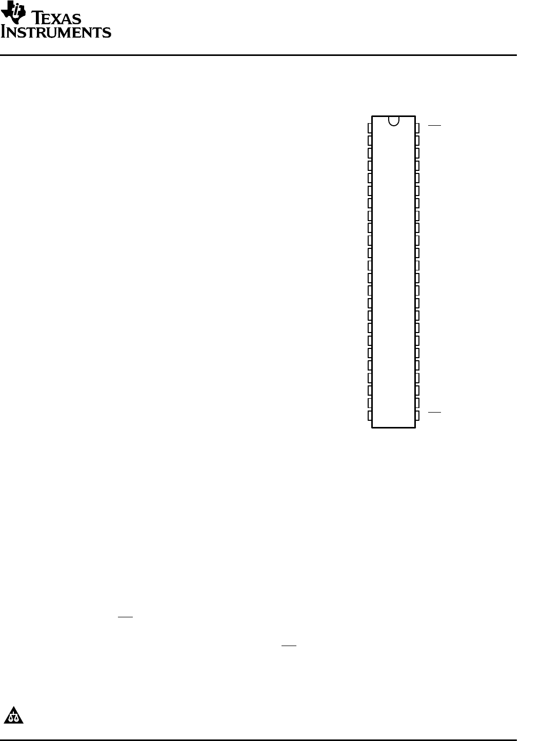
DL PACKAGE
(TOP VIEW)
1
2
3
4
5
6
7
8
9
10
11
12
13
14
15
16
17
18
19
20
21
22
23
24
48
47
46
45
44
43
42
41
40
39
38
37
36
35
34
33
32
31
30
29
28
27
26
25
1DIR
1B1
1B2
GND
1B3
1B4
V
CC
1B5
1B6
GND
1B7
1B8
2B1
2B2
GND
2B3
2B4
V
CC
2B5
2B6
GND
2B7
2B8
2DIR
1OE
1A1
1A2
GND
1A3
1A4
V
CC
1A5
1A6
GND
1A7
1A8
2A1
2A2
GND
2A3
2A4
V
CC
2A5
2A6
GND
2A7
2A8
2OE
DESCRIPTION/ORDERING INFORMATION
SN74ABT16245A-EP
16-BIT BUS TRANSCEIVER
WITH 3-STATE OUTPUTS
SCBS807B OCTOBER 2005 REVISED JANUARY 2006
Controlled Baseline
One Assembly/Test Site, One Fabrication
Site
Enhanced Diminishing Manufacturing
Sources (DMS) Support
Enhanced Product-Change Notification
Qualification Pedigree
(1)
Member of the Texas Instruments
Widebus™ Family
State-of-the-Art EPIC-IIB™ BiCMOS Design
Significantly Reduces Power Dissipation
Typical V
OLP
(Output Ground Bounce) <1 V at
V
CC
= 5 V, T
A
= 25 ° C
High-Impedance State During Power Up and
Power Down
Distributed V
CC
and GND Pin Configuration
Minimizes High-Speed Switching Noise
Flow-Through Architecture Optimizes PCB
Layout
High-Drive Outputs (–32-mA I
OH
, 64-mA I
OL
)
Latch-Up Performance Exceeds 500 mA Per
JESD 70
ESD Protection Exceeds 2000 V Per
MIL-STD-883, Method 3015; Exceeds 200 V
Using Machine Model (C = 200 pF, R = 0)
Shrink Small-Outline (DL) Package
(1) Component qualification in accordance with JEDEC and
industry standards to ensure reliable operation over an
extended temperature range. This includes, but is not limited
to, Highly Accelerated Stress Test (HAST) or biased 85/85,
temperature cycle, autoclave or unbiased HAST,
electromigration, bond intermetallic life, and mold compound
life. Such qualification testing should not be viewed as
justifying use of this component beyond specified
performance and environmental limits.
The SN74ABT16245A-EP is a 16-bit noninverting 3-state transceiver designed for synchronous two-way
communication between data buses. The control-function implementation minimizes external timing
requirements.
This device can be used as two 8-bit transceivers or one 16-bit transceiver. It allows data transmission from the
A bus to the B bus or from the B bus to the A bus, depending on the logic level at the direction-control (DIR)
input. The output-enable ( OE) input can be used to disable the device so that the buses are effectively isolated.
When V
CC
is between 0 and 2.1 V, the device is in the high-impedance state during power up or power down.
However, to ensure the high-impendance state above 2.1 V, OE should be tied to V
CC
through a pullup resistor;
the minimum value of the resistor is determined by the current-sinking capability of the driver.
The SN74ABT16245A-EP is characterized for operation from –55 ° C to 125 ° C.
Please be aware that an important notice concerning availability, standard warranty, and use in critical applications of Texas
Instruments semiconductor products and disclaimers thereto appears at the end of this data sheet.
Widebus, EPIC-IIB are trademarks of Texas Instruments.
PRODUCTION DATA information is current as of publication date.
Copyright © 2005–2006, Texas Instruments Incorporated
Products conform to specifications per the terms of the Texas
Instruments standard warranty. Production processing does not
necessarily include testing of all parameters.
www.ti.com
1A2
46
1A3
44
1A4
43
1A5
41
1A6
40
1A7
38
1A8
37
2A2
35
2A3
33
2A4
32
2A5
30
2A6
29
2A7
27
2A8
26
1OE
2OE
1A1
47
G3
48
3 EN1 [BA]
1
1DIR
3 EN2 [AB]
G6
25
6 EN4 [BA]
24
2DIR
6 EN5 [AB]
1B1
2
1B2
3
1B3
5
1B4
6
1B5
8
1B6
9
1B7
11
1B8
12
2A1
36
2B1
13
2B2
14
2B3
16
2B4
17
2B5
19
2B6
20
2B7
22
2B8
23
1
2
4
5
SN74ABT16245A-EP
16-BIT BUS TRANSCEIVER
WITH 3-STATE OUTPUTS
SCBS807B OCTOBER 2005 REVISED JANUARY 2006
ORDERING INFORMATION
T
A
PACKAGE
(1)
ORDERABLE PART NUMBER TOP-SIDE MARKING
–55 ° C to 125 ° C SSOP DL Reel of 1000 CABT16245AMDLREP ABT16245AMEP
(1) Package drawings, standard packing quantities, thermal data, symbolization, and PCB design guidelines are available at
www.ti.com/sc/package.
FUNCTION TABLE
(EACH 8-BIT SECTION)
INPUTS
OPERATION
OE DIR
L L B data to A bus
L H A data to B bus
H X Isolation
LOGIC SYMBOL
(1)
(1) This symbol is in accordance with ANSI/IEEE Std 91-1984 and IEC Publication 617-12.
2
www.ti.com
To Seven Other Channels
1DIR
1A1
1B1
1OE
To Seven Other Channels
2DIR
2A1
2B1
2OE
1
47
24
36
48
2
25
13
Absolute Maximum Ratings
(1)
Recommended Operating Conditions
(1)
SN74ABT16245A-EP
16-BIT BUS TRANSCEIVER
WITH 3-STATE OUTPUTS
SCBS807B OCTOBER 2005 REVISED JANUARY 2006
LOGIC DIAGRAM (POSITIVE LOGIC)
over operating free-air temperature range (unless otherwise noted)
MIN MAX UNIT
V
CC
Supply voltage range –0.5 7 V
V
I
Input voltage range (except I/O ports)
(2)
–0.5 7 V
V
O
Voltage range applied to any output in the high or power-off state –0.5 5.5 V
I
O
Current into any output in the low state 96 mA
I
IK
Input clamp current V
I
< 0 –18 mA
I
OK
Output clamp current V
O
< 0 –50 mA
θ
JA
Package thermal impedance
(3)
94 ° C/W
T
stg
Storage temperature range –65 150 ° C
(1) Stresses beyond those listed under "absolute maximum ratings" may cause permanent damage to the device. These are stress ratings
only, and functional operation of the device at these or any other conditions beyond those indicated under "recommended operating
conditions" is not implied. Exposure to absolute-maximum-rated conditions for extended periods may affect device reliability.
(2) The input and output negative-voltage ratings may be exceeded if the input and output clamp-current ratings are observed.
(3) The package thermal impedance is calculated in accordance with JESD 51.
MIN MAX UNIT
V
CC
Supply voltage 4.5 5.5 V
V
IH
High-level input voltage 2 V
V
IL
Low-level input voltage 0.8 V
V
I
Input voltage 0 V
CC
V
I
OH
High-level output current –24 mA
I
OL
Low-level output current 48 mA
t/ v Input transition rise or fall rate Outputs enabled 10 ns/V
t/ V
CC
Power-up ramp rate 200 µ s/V
T
A
Operating free-air temperature –55 125 ° C
(1) All unused inputs of the device must be held at V
CC
or GND to ensure proper device operation. Refer to the TI application report,
Implications of Slow or Floating CMOS Inputs, literature number SCBA004.
3
1234NEXT