Closed Dec 25th-26th
800-300-1968
We Stock Hard to Find Parts
My Account
|
My Orders
|
My Cart
Questions?
(800) 300-1968
Register
(current)
My Account
(current)
My Orders
(current)
My Cart
(current)
Categories
(current)
Manufacturers
Request a Quote
Sell Your Excess
Consignment
Quality Assurance
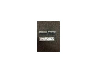
74F374SC
Part #
74F374SC
Description
Category
IC
Availability
Out of Stock
Qty
0
Qty
Price
1 +
$1.42704
Related Items
Fairchild Semiconductor
IC
74F373
$0.57531
SIGNETICS
IC
74F373N
$0.14388
Fairchild Semiconductor
IC
74F373PC
$0.62444
SIGNETICS
IC
74F374/B
$7.33998
Fairchild Semiconductor
IC
74F374DC
$10.10745
SIGNETICS
IC
74F374N
$0.54675