Closed Dec 25th-26th
800-300-1968
We Stock Hard to Find Parts
My Account
|
My Orders
|
My Cart
Questions?
(800) 300-1968
Register
(current)
My Account
(current)
My Orders
(current)
My Cart
(current)
Categories
(current)
Manufacturers
Request a Quote
Sell Your Excess
Consignment
Quality Assurance
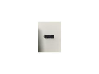
9602DM
Part #
9602DM
Description
Category
IC
Availability
In Stock
Qty
1
Qty
Price
1 +
$3.31185
Manufacturer
Available
Qty
Fairchild Semiconductor
Date Code: 8026
Freelance Stock:
1
Ships Immediately
Add to Cart
Related Items
Advanced Micro Devices
IC
9602DM-B
National Semiconductor Corp
IC
9602DMQB
$6.42886
Fairchild Semiconductor
IC
008-25424
$11.58351
Harris Corporation
IC
01-6945-9
Motorola Corp
IC
010-143121-0002
Texas Instruments
IC
01295-672141D