559
XC6367/6368
Series
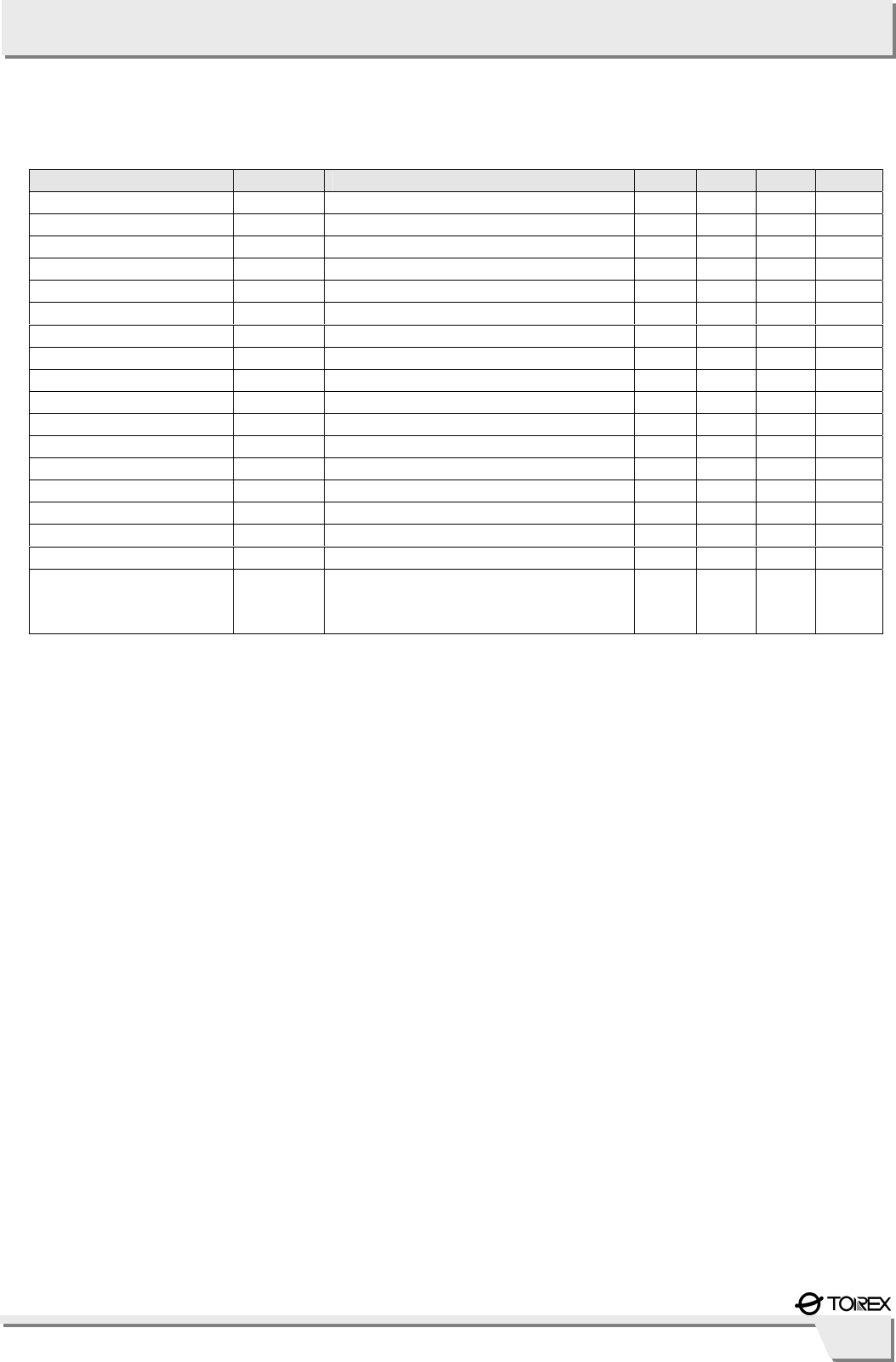
PARAMETER SYMBOL CONDITIONS MIN. TYP. MAX. UNITS
Output Voltage VOUT 4875 5.000 5.125 V
Supply Voltage (* 1) VDD 2.0 - 10.0 V
Maximum Input Voltage VIN 10.0 - - V
Oscillation Start Voltage 1 VST1 Tr: 2SD1628, IOUT=1.0mA - - 0.9 V
Oscillation Start Voltage 2 VST2 VOUT=CE : Apply voltage - - 0.8 V
Oscillation Hold Voltage VHLD Tr: 2SD1628, IOUT=1.0mA - - 0.7 V
Supply Current 1 IDD1 VOUT=CE=setting output voltage x 0.95 - 180 280
μA
Supply Current 2 IDD2 VOUT=CE=setting output voltage + 0.5V - 22 38
μA
Stand-by Current ISTB VOUT=setting output voltage x 0.95, CE=0V - - 0.5
μA
Oscillation Frequency FOSC Same as IDD1 255 300 345 kHz
Maximum Duty Ratio MAXDTY Same as IDD1 78 85 92 %
PFM Duty Ratio (* 3) PFMDTY IOUT=0mA 15 25 35 %
CE "High" Voltage VCEH VOUT=setting output voltage x0.95 0.65 - - V
CE "Low" Voltage VCEL VOUT=setting output voltage x0.95 - - 0.20 V
EXT "High" ON Resistance REXTH Same as IDD1, VEXT=VOUT-0.4V - 20 29
Ω
EXT "Low" ON Resistance REXTL Same as IDD1, VEXT=0.4V - 13 19
Ω
Efficiency (* 2) EFFI - 87 - %
Soft-Start Time TSS
Connect R
SS and CSS,
CE:0V→3.0V
(XC6367C/F and XC6368C/F series)
5 10 20 msec
XC6367A503MR, XC6368A503MR
Conditions: Unless otherwise specified, connect VDD to VOUT; VIN=setting output voltage x 0.6, IOUT=200mA
NOTE:
* 1: When taking V
DD from another power source please ensure that VDD = 2.0V or more.
Oscillation will occur with a value of V
DD = 0.8V or more, but with a value of VDD = 2.0V or more,
output voltage and oscillation frequency will be stable.
* 2: EFFI = {[(output voltage) x (output current)]÷[(input voltage) x (input current)] x 100
* 3: Applies to the XC6368 series only (duty ratio when control changes to PFM).
* 4: The values of supply voltage and NOTE *1 do not apply to XC6367E/F and XC6368E/F series. For XC6367E/F and
XC6368E/F series, output voltage less than 2.0V cannot be set-up.
VOUT=5.0V, FOSC=300kHz,Ta=25℃
■ELECTRICAL CHARACTERISTICS (Continued)


