4
PARAMETER TEST CONDITION
UC1842/3/4/5
UC2842/3/4/5
UC3842/3/4/5 UNITS
MIN TYP MAX MIN TYP MAX
Output Section
Output Low Level I
SINK = 20mA 0.1 0.4 0.1 0.4 V
I
SINK = 200mA 1.5 2.2 1.5 2.2 V
Output High Level I
SOURCE = 20mA 13 13.5 13 13.5 V
I
SOURCE = 200mA 12 13.5 12 13.5 V
Rise Time T
J = 25°C, CL = 1nF (Note 2) 50 150 50 150 ns
Fall Time T
J = 25°C, CL = 1nF (Note 2) 50 150 50 150 ns
Under-voltage Lockout Section
Start Threshold X842/4 15 16 17 14.5 16 17.5 V
X843/5 7.8 8.4 9.0 7.8 8.4 9.0 V
Min. Operating Voltage
After Turn On
X842/4 9 10 11 8.5 10 11.5 V
X843/5 7.0 7.6 8.2 7.0 7.6 8.2 V
PWM Section
Maximum Duty Cycle X842/3 95 97 100 95 97 100 %
X844/5 46 48 50 47 48 50 %
Minimum Duty Cycle 0 0 %
Total Standby Current
Start-Up Current 0.5 1 0.5 1 mA
Operating Supply Current V
PIN 2 =VPIN 3 =0V 1117 1117mA
V
CC Zener Voltage ICC = 25mA 30 34 30 34 V
Note 2: These parameters, although guaranteed, are not 100% tested in production.
Note 3: Parameter measured at trip point of latch with V
PIN 2 =0
.
Note 4: Gain defined as:
A
VPIN
VPIN
VPIN V=≤≤
∆
∆
1
3
0308;.
.
Note 5: Adjust V
CC above the start threshold before setting at 15V.
Note 6: Output frequency equals oscillator frequency for the UC1842 and UC1843.
Output frequency is one half oscillator frequency for the UC1844 and UC1845.
UC1842/3/4/5
UC2842/3/4/5
UC3842/3/4/5
ELECTRICAL CHARACTERISTICS:
Unless otherwise stated, these specifications apply for −55°C
≤
TA
≤
125°C for the
UC184X; −40°C
≤
T
A
≤
85°C for the UC284X; 0°C
≤
TA
≤
70°C for the 384X; VCC =
15V (Note 5); R
T = 10k; CT = 3.3nF, TA=TJ.
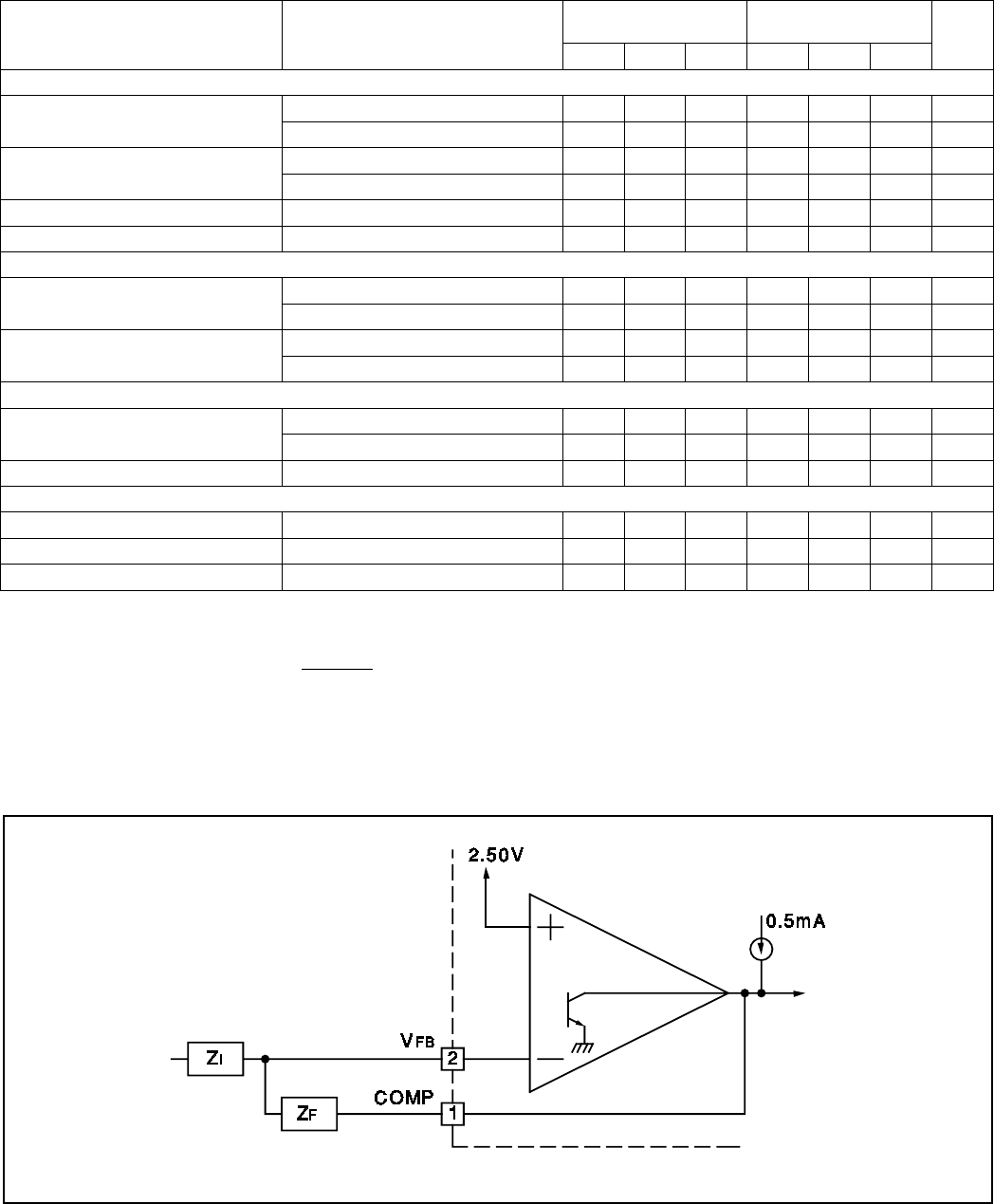
ERROR AMP CONFIGURATION
Error Amp can Source or Sink up to 0.5mA


