Closed Dec 25th-26th
800-300-1968
We Stock Hard to Find Parts
My Account
|
My Orders
|
My Cart
Questions?
(800) 300-1968
Register
(current)
My Account
(current)
My Orders
(current)
My Cart
(current)
Categories
(current)
Manufacturers
Request a Quote
Sell Your Excess
Consignment
Quality Assurance
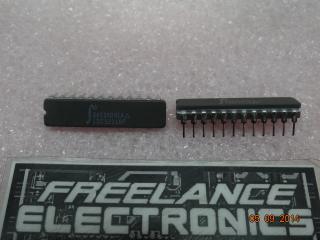
8403602JA
Part #
8403602JA
Description
SRAM ASYNC SGL 5V 16KBIT 2KX890NS 24CDIP - Rail/Tube
Category
IC
Availability
In Stock
Qty
5
Qty
Price
1 - 1
$156.56096
2 - 2
$124.53713
3 - 3
$117.42072
4 +
$109.11825
Manufacturer
Available
Qty
Harris Corporation
Date Code: 9304
Freelance Stock:
5
Ships Immediately
Add to Cart
Related Items
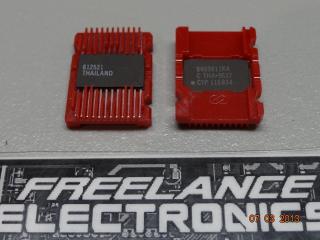
Integrated Device Technology
IC
84036083A
$90.47163
Integrated Device Technology
IC
8403609LA
$18.97495
Integrated Device Technology
IC
8403611JA
$18.42286
CYPRESS SEMICONDUCTOR
IC
8403611KA
$960.15042
Integrated Device Technology
IC
8403611LA
$17.48586
Integrated Device Technology
IC
8403613JA
$35.60226