Closed Dec 25th-26th
800-300-1968
We Stock Hard to Find Parts
My Account
|
My Orders
|
My Cart
Questions?
(800) 300-1968
Register
(current)
My Account
(current)
My Orders
(current)
My Cart
(current)
Categories
(current)
Manufacturers
Request a Quote
Sell Your Excess
Consignment
Quality Assurance
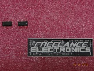
74VHC393M
Part #
74VHC393M
Description
COUNTER/DIVIDER DUAL 4BIT BINARY UP 14SOIC N - Rail/Tube
Category
IC
Availability
In Stock
Qty
3
Qty
Price
1 +
$0.20285
Manufacturer
Available
Qty
Fairchild Semiconductor
Freelance Stock:
3
Ships Immediately
Add to Cart
Related Items
National Semiconductor Corp
IC
74VHC08M
$0.14697
Fairchild Semiconductor
IC
74VHC08MTC
$0.03420
Fairchild Semiconductor
IC
74VHC08MTCX
$0.04615
SGS Thomson
IC
74VHC08TTR
$0.84860
Fairchild Semiconductor
IC
74VHC123AM
$0.14575
National Semiconductor Corp
IC
74VHC123AN
$0.11932