Closed Dec 25th-26th
800-300-1968
We Stock Hard to Find Parts
My Account
|
My Orders
|
My Cart
Questions?
(800) 300-1968
Register
(current)
My Account
(current)
My Orders
(current)
My Cart
(current)
Categories
(current)
Manufacturers
Request a Quote
Sell Your Excess
Consignment
Quality Assurance
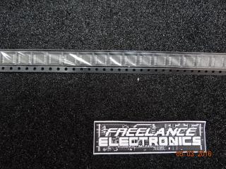
74LVC125D
Part #
74LVC125D
Description
Category
IC
Availability
In Stock
Qty
78
Manufacturer
Available
Qty
Philips Semiconductor
Date Code: 9519
Freelance Stock:
78
Ships Immediately
Request For Quote
Request For Quote
Related Items
Philips Semiconductor
IC
74LVC00A
$0.85810
Philips Semiconductor
IC
74LVC00AD
$0.05868
Philips Semiconductor
IC
74LVC08AD
$0.05480
Philips Semiconductor
IC
74LVC08AD-T
$0.46744
Philips Semiconductor
IC
74LVC11PW
$0.15655
Philips Semiconductor
IC
74LVC125AD
$0.10281