Closed Dec 25th-26th
800-300-1968
We Stock Hard to Find Parts
My Account
|
My Orders
|
My Cart
Questions?
(800) 300-1968
Register
(current)
My Account
(current)
My Orders
(current)
My Cart
(current)
Categories
(current)
Manufacturers
Request a Quote
Sell Your Excess
Consignment
Quality Assurance
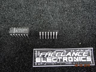
74LS533N
Part #
74LS533N
Description
Category
IC
Availability
In Stock
Qty
36
Qty
Price
1 - 7
$2.33369
8 - 15
$1.85635
16 - 22
$1.75027
23 - 30
$1.62651
31 +
$1.44972
Manufacturer
Available
Qty
SIGNETICS
Freelance Stock:
36
Ships Immediately
Add to Cart
Related Items
Fairchild Semiconductor
IC
74LS502PC
$3.92672
SIGNETICS
IC
74LS51N
$0.54060
SIGNETICS
IC
74LS534N
$4.52030
Philips Semiconductor
IC
74LS54
$4.08743
SIGNETICS
IC
74LS540N
$5.05377
SIGNETICS
IC
74LS541N
$1.36979