Closed Dec 25th-26th
800-300-1968
We Stock Hard to Find Parts
My Account
|
My Orders
|
My Cart
Questions?
(800) 300-1968
Register
(current)
My Account
(current)
My Orders
(current)
My Cart
(current)
Categories
(current)
Manufacturers
Request a Quote
Sell Your Excess
Consignment
Quality Assurance
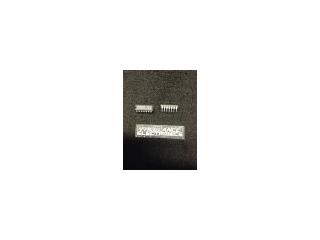
74HC08AP
Part #
74HC08AP
Description
Category
IC
Availability
Out of Stock
Qty
0
Related Items
TOSHIBA
IC
74HC00AP
$0.76490
NXP SEMICONDUCTORS
IC
74HC00D
$0.05480
Philips Semiconductor
IC
74HC00N
$0.18940
Philips Semiconductor
IC
74HC02D
$0.04116
Philips Semiconductor
IC
74HC02N
$0.20552
Fairchild Semiconductor
IC
74HC04AP
$0.15827