Freelance Electronics Components Distributor
Closed Dec 25th-26th
800-300-1968
We Stock Hard to Find Parts

74F538PC

Part # 74F538PC
Description Decoder/Demultiplexer Single3-to-8 20-Pin PDIP W Rail
Category IC
Availability In Stock
Qty 9
Qty Price
1 + $1.66577
Manufacturer Available Qty
National Semiconductor Corp
Date Code: 9003
  • Shipping Freelance Stock: 9
    Ships Immediately


Technical Document


DISCLAIMER: The information provided herein is solely for informational purposes. Customers must be aware of the suitability of this product for their application, and consider that variable factors such as Manufacturer, Product Category, Date Codes, Pictures and Descriptions may differ from available inventory.

© 2004 Fairchild Semiconductor Corporation DS009551 www.fairchildsemi.com
April 1988
Revised January 2004
74F538 1-of-8 Decoder with 3-STATE Outputs
74F538
1-of-8 Decoder with 3-STATE Outputs
General Description
The 74F538 decoder/demultiplexer accepts three Address
(A
0
–A
2
) input signals and decodes them to select one of
eight mutually exclusive outputs. A polarity control input (P)
determines whether the outputs are active LOW or active
HIGH. A HIGH Signal on either of the active LOW Output
Enable (OE
) inputs forces all outputs to the high imped-
ance state. Two active HIGH and two active LOW input
enables are available for easy expansion to 1-of 32 decod-
ing with four packages, or for data demultiplexing to 1-of-8
or 1-of-16 destinations.
Features
Output polarity control
Data demultiplexing capability
Multiple enables for expansion
3-STATE outputs
Ordering Code:
Devices also available in Tape and Reel. Specify by appending the suffix letter X to the ordering code.
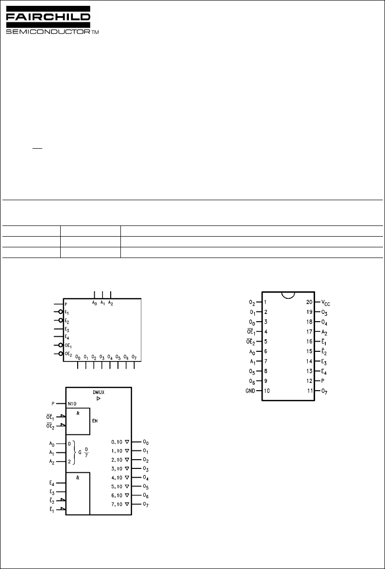
Logic Symbols
IEEE/IEC
Connection Diagram
Order Number Package Number Package Description
74F538SC M20B 20-Lead Small Outline Integrated Circuit (SOIC), JEDEC MS-013, 0.300" Wide
74F538PC N20A 20-Lead Plastic Dual-In-Line Package (PDIP), JEDEC MS-001, 0.300" Wide
www.fairchildsemi.com 2
74F538
Unit Loading/Fan Out
Truth Table
H = HIGH Voltage Level
L = LOW Voltage Level
X = Immaterial
Z = High Impedance
Pin Names Description
U.L.
Input I
IH
/I
IL
HIGH/LOW
Output I
OH
/I
OL
A
0
A
2
Address Inputs 1.0/1.0 20 µA/0.6 mA
E
1
, E
2
Enable Inputs (Active LOW) 1.0/1.0 20 µA/0.6 mA
E
3
, E
4
Enable Inputs (Active HIGH) 1.0/1.0 20 µA/0.6 mA
P Polarity Control Input 1.0/1.0 20
µA/0.6 mA
OE
1
, OE
2
Output Enable Inputs (Active LOW) 1.0/1.0 20 µA/0.6 mA
O
0
O
7
3-STATE Outputs 150/40 (33.3) 3 mA/24 mA (20 mA)
Function
Inputs Outputs
OE
1
OE
2
E
1
E
2
E
3
E
4
A
2
A
1
A
0
O
0
O
1
O
2
O
3
O
4
O
5
O
6
O
7
High H X XXXXXXXZZZZZZZZ
Impedance X H XXXXXXXZZZZZZZZ
Disable L L HXXXXXX
L L XHXXXXX
Outputs Equal P Input
L L XXLXXXX
L L XXXLXXX
Active HIGH L L LLHHLLLHLLLLLLL
Output L L LLHHLLHLHLLLLLL
(P
= L) L L LLHHLHLLLHLLLLL
L L LLHHLHHLLLHLLLL
L L LLHHHLLLLLLHLLL
L L LLHHHLHLLLLLHLL
L L LLHHHHLLLLLLLHL
L L LLHHHHHLLLLLLLH
Active LOW L L LLHHLL L LHHHHHHH
Output L L LLHHLLHHLHHHHHH
(P
= H) L L L LHHLHLHHLHHHHH
L L LLHHLHHHHHLHHHH
L L LLHHHL LHHHHLHHH
L L L LHHHLHHHHHHLHH
L L L LHHHHLHHHHHHLH
L L L LHHHHHHHHHHHHL
3 www.fairchildsemi.com
74F538
Logic Diagram
Please note that this diagram is provided only for the understanding of logic operations and should not be used to estimate propagation delays.
123NEXT