Freelance Electronics Components Distributor
Closed Dec 25th-26th
800-300-1968
We Stock Hard to Find Parts

74F534D

Part # 74F534D
Description
Category IC
Availability Out of Stock
Qty 0
Qty Price
1 + $0.37000


Technical Document


DISCLAIMER: The information provided herein is solely for informational purposes. Customers must be aware of the suitability of this product for their application, and consider that variable factors such as Manufacturer, Product Category, Date Codes, Pictures and Descriptions may differ from available inventory.

Philips Semiconductors Product specification
74F533,* 74F534Latch/flip-flop
1999 Jan 08
4
* Discontinued part. Please see the Discontinued Products List.
LOGIC DIAGRAM – 74F533
D0 D1 D2 D3 D4 D5 D6 D7
Q
0Q1Q2Q3Q4Q5Q6Q7
E
OE
3 4 7 8 13 14 17 18
191615129652
1
11
E
D
Q E
D
Q EQ
D
E
D
Q E
D
Q E
D
Q E
D
Q E
D
Q
V
CC
=Pin 20
GND=Pin 10
SF00987
LOGIC DIAGRAM – 74F534
D0 D1 D2 D3 D4 D5 D6 D7
Q
0Q1Q2Q3Q4Q5Q6Q7
CP
OE
3 4 7 8 13 14 17 18
191615129652
1
11
CP
D
Q CP
D
Q CP Q
D
CP
D
Q CP
D
Q CP
D
Q CP
D
Q CP
D
Q
V
CC
=Pin 20
GND=Pin 10
SF00988
FUNCTION TABLE – 74F533
INPUTS
INTERNAL
OUTPUTS
OPERATING MODES
OE E Dn
REGISTER
Q0 – Q7
OPERATING
MODES
L
L
H
H
L
H
L
H
H
L
Load and read register
L
L
l
h
L
H
H
L
Enable and read register
L L X NC NC Hold
H
H
L
H
X
Dn
NC
Dn
Z
Z
Disable outputs
H = High voltage level
h = High voltage level one setup time prior to the High-to-Low E transition
L = Low voltage level
l = Low voltage level one setup time prior to the High-to-Low E transition
NC= No change
X = Don’t care
Z = High impedance “off” state
= High-to-Low E transition
Philips Semiconductors Product specification
74F533,* 74F534Latch/flip-flop
1999 Jan 08
5
* Discontinued part. Please see the Discontinued Products List.
FUNCTION TABLE – 74F534
INPUTS
INTERNAL
OUTPUTS
OPERATING MODES
OE CP Dn
REGISTER
Q0 – Q7
OPERATING
MODES
L
L
l
h
L
H
H
L
Load and read register
L X NC NC Hold
H
H
X
Dn
NC
Dn
Z
Z
Disable outputs
H = High voltage level
h = High voltage level one setup time prior to the Low-to-High clock transition
L = Low voltage level
l = Low voltage level one setup time prior to the Low-to-High clock transition
NC= No change
X = Don’t care
Z = High impedance “off” state
= Low-to-High clock transition
= Not a Low-to-High clock transition
ABSOLUTE MAXIMUM RATINGS
(Operation beyond the limits set forth in this table may impair the useful life of the device.
Unless otherwise noted these limits are over the operating free-air temperature range.)
SYMBOL PARAMETER RATING UNIT
V
CC
Supply voltage –0.5 to +7.0 V
V
IN
Input voltage –0.5 to +7.0 V
I
IN
Input current –30 to +5.0 mA
V
OUT
Voltage applied to output in High output state –0.5 to +V
CC
V
I
OUT
Current applied to output in Low output state 48 mA
T
amb
Operating free-air temperature range 0 to +70 °C
T
stg
Storage temperature –65 to +125 °C
RECOMMENDED OPERATING CONDITIONS
SYMBOL
PARAMETER
LIMITS
UNIT
SYMBOL
PARAMETER
MIN NOM MAX
UNIT
V
CC
Supply voltage 4.5 5.0 5.5 V
V
IH
High-level input voltage 2.0 V
V
IL
Low-level input voltage 0.8 V
I
IK
Input clamp current –18 mA
I
OH
High-level output current –3 mA
I
OL
Low-level output current 24 mA
T
amb
Operating free-air temperature range 0 70 °C
Philips Semiconductors Product specification
74F533,* 74F534Latch/flip-flop
1999 Jan 08
6
* Discontinued part. Please see the Discontinued Products List.
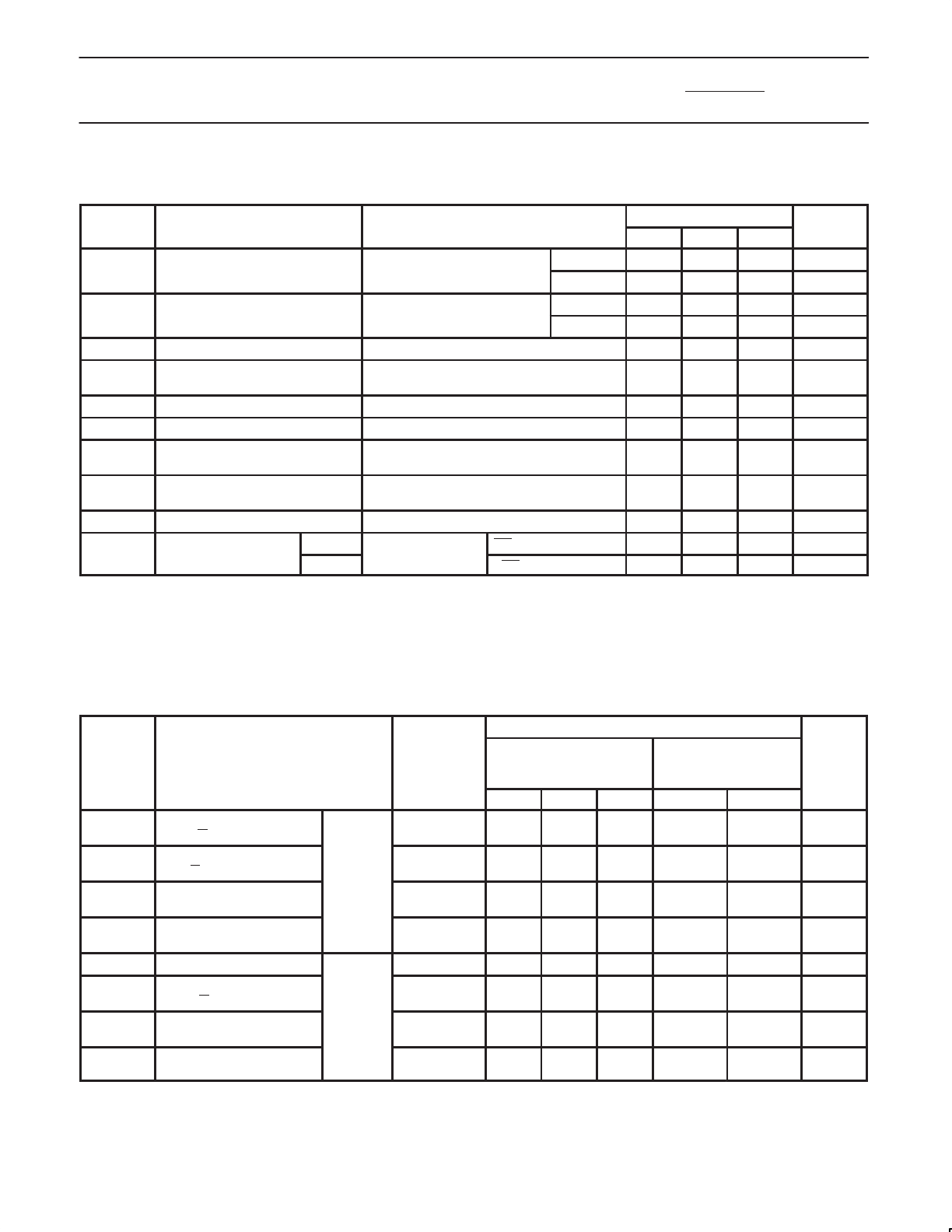
DC ELECTRICAL CHARACTERISTICS
(Over recommended operating free-air temperature range unless otherwise noted.)
SYMBOL
PARAMETER
TEST CONDITIONS
1
LIMITS
UNIT
SYMBOL
PARAMETER
TEST
CONDITIONS
1
MIN TYP
2
MAX
UNIT
V
O
High level out
p
ut voltage
V
CC
= MIN
,
V
IL
= MAX
,
±10%V
CC
2.4 V
V
OH
High
-
le
v
el
o
u
tp
u
t
v
oltage
V
CC
MIN,
V
IL
MAX,
V
IH
= MIN, I
OH
= MAX
±5%V
CC
2.7 3.3 V
V
O
Low level out
p
ut voltage
V
CC
= MIN
,
V
IL
= MAX
,
±10%V
CC
0.35 0.50 V
V
OL
Lo
w-
le
v
el
o
u
tp
u
t
v
oltage
V
CC
MIN,
V
IL
MAX,
V
IH
= MIN, I
OL
= MAX
±5%V
CC
0.35 0.50 V
V
IK
Input clamp voltage V
CC
= MIN, I
I
= I
IK
–0.73 –1.2 V
I
I
Input current at
maximum input voltage
V
CC
= MAX, V
I
= 7.0V 100 µA
I
IH
High-level input current V
CC
= MAX, V
I
= 2.7V 20 µA
I
IL
Low-level input current V
CC
= MAX, V
I
= 0.5V –0.6 mA
I
OZH
Off-state output current,
High-level voltage applied
V
CC
= MAX, V
O
= 2.7V 50 µA
I
OZL
Off-state output current,
Low-level voltage applied
V
CC
= MAX, V
O
= 0.5V –50 µA
I
OS
Short-circuit output current
3
V
CC
= MAX –60 –150 mA
I
CC
Su
pp
ly current (total)
74F533
V
CC
= MAX
OE=4.5V, Dn=E=GND 41 61 mA
I
CC
S
u
ppl
y
c
u
rrent
(total)
74F534
V
CC
=
MAX
OE=4.5V, Dn=GND 51 86 mA
NOTES:
1. For conditions shown as MIN or MAX, use the appropriate value specified under recommended operating conditions for the applicable type.
2. All typical values are at V
CC
= 5V, T
amb
= 25°C.
3. Not more than one output should be shorted at a time. For testing I
OS
, the use of high-speed test apparatus and/or sample-and-hold
techniques are preferable in order to minimize internal heating and more accurately reflect operational values. Otherwise, prolonged shorting
of a High output may raise the chip temperature well above normal and thereby cause invalid readings in other parameter tests. In any
sequence of parameter tests, I
OS
tests should be performed last.
AC ELECTRICAL CHARACTERISTICS
LIMITS
SYMBOL PARAMETER
TEST
CONDITIONS
T
amb
= +25°C
V
CC
= +5V
C
L
= 50pF, R
L
= 500
T
amb
= 0°C to +70°C
V
CC
= +5V ± 10%
C
L
= 50pF, R
L
= 500
UNIT
MIN TYP MAX MIN MAX
t
PLH
t
PHL
Propagation delay
Dn to Qn
Waveform 2
4.0
3.0
6.0
4.5
8.5
7.0
4.0
3.0
9.5
8.0
ns
t
PLH
t
PHL
Propagation delay
E to Qn
Waveform 3
5.0
3.0
6.5
4.5
9.5
7.0
5.0
3.0
10.0
8.0
ns
t
PZH
t
PZL
Output Enable time
to High or Low level
Waveform 6
Waveform 7
2.0
2.0
4.5
5.0
7.0
7.0
2.0
2.0
8.0
8.0
ns
t
PHZ
t
PLZ
Output Disable time
from High or Low level
Waveform 6
Waveform 7
2.0
2.0
3.5
3.0
6.0
5.5
2.0
2.0
7.0
6.5
ns
f
MAX
Maximum Clock frequency Waveform 1 150 165 135 MHz
t
PLH
t
PHL
Propagation delay
CP to Qn
Waveform 1
3.0
3.0
4.5
4.5
7.0
7.0
2.5
2.5
7.5
7.5
ns
t
PZH
t
PZL
Output Enable time
to High or Low level
74F534
Waveform 6
Waveform 7
2.0
2.0
4.5
5.0
7.5
7.5
2.0
2.0
8.5
8.5
ns
t
PHZ
t
PLZ
Output Disable time
from High or Low level
Waveform 6
Waveform 7
2.0
2.0
3.5
3.5
6.5
5.5
2.0
2.0
7.5
6.5
ns
PREVIOUS1234NEXT