Closed Dec 25th-26th
800-300-1968
We Stock Hard to Find Parts
My Account
|
My Orders
|
My Cart
Questions?
(800) 300-1968
Register
(current)
My Account
(current)
My Orders
(current)
My Cart
(current)
Categories
(current)
Manufacturers
Request a Quote
Sell Your Excess
Consignment
Quality Assurance
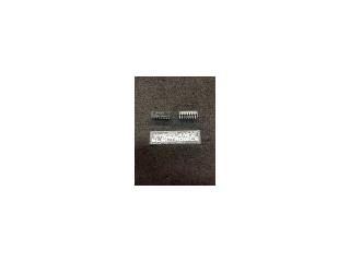
74F257A
Part #
74F257A
Description
Category
IC
Availability
Out of Stock
Qty
0
Qty
Price
1 +
$1.14163
Related Items
National Semiconductor Corp
IC
74F251APC
$0.12785
Fairchild Semiconductor
IC
74F251PC
$18.79424
National Semiconductor Corp
IC
74F253DC
$12.72913
SIGNETICS
IC
74F253N
$0.20272
National Semiconductor Corp
IC
74F253PC
$0.12785
National Semiconductor Corp
IC
74F257AD
$0.58761