Closed Dec 25th-26th
800-300-1968
We Stock Hard to Find Parts
My Account
|
My Orders
|
My Cart
Questions?
(800) 300-1968
Register
(current)
My Account
(current)
My Orders
(current)
My Cart
(current)
Categories
(current)
Manufacturers
Request a Quote
Sell Your Excess
Consignment
Quality Assurance
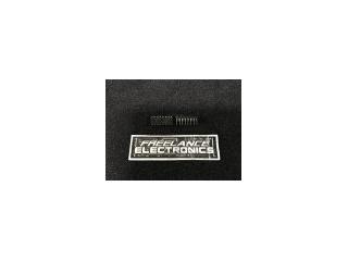
74F154D
Part #
74F154D
Description
Category
IC
Availability
Out of Stock
Qty
0
Qty
Price
1 +
$0.36000
Related Items
Fairchild Semiconductor
IC
74F151ADC
$0.89630
Fairchild Semiconductor
IC
74F151APC
$0.29843
Fairchild Semiconductor
IC
74F151ASC
$0.19784
SIGNETICS
IC
74F151N
$0.45262
Fairchild Semiconductor
IC
74F151PC
$0.50980
Fairchild Semiconductor
IC
74F153DC
$0.14123