Closed Dec 25th-26th
800-300-1968
We Stock Hard to Find Parts
My Account
|
My Orders
|
My Cart
Questions?
(800) 300-1968
Register
(current)
My Account
(current)
My Orders
(current)
My Cart
(current)
Categories
(current)
Manufacturers
Request a Quote
Sell Your Excess
Consignment
Quality Assurance
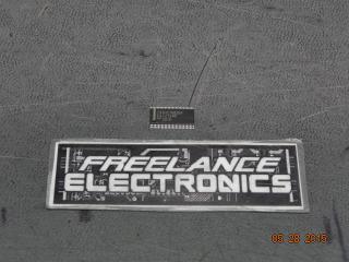
74AVCM162834DGG
Part #
74AVCM162834DGG
Description
IC TRANSCVR 3-ST 18BIT 56TSSOP
Category
IC
Availability
In Stock
Qty
39
Qty
Price
1 - 8
$13.09623
9 - 16
$10.41746
17 - 24
$9.82218
25 - 32
$9.12768
33 +
$8.13554
Manufacturer
Available
Qty
Philips Semiconductor
Date Code: 9927
Freelance Stock:
10
Ships Immediately
Philips Semiconductor
Date Code: 9927
Freelance Stock:
29
Ships Immediately
Add to Cart
Related Items
Philips Semiconductor
IC
74AVC16334ADGG
$12.43165
Philips Semiconductor
IC
74AVC16834ADGG
$12.59767
Philips Semiconductor
IC
74AVC16834DGG
$8.32747
Philips Semiconductor
IC
74AVC16835DGG
$14.95417
Philips Semiconductor
IC
74AVC16836ADGG
$12.23526
Philips Semiconductor
IC
74AVC16836DGG
$13.61003