Closed Dec 25th-26th
800-300-1968
We Stock Hard to Find Parts
My Account
|
My Orders
|
My Cart
Questions?
(800) 300-1968
Register
(current)
My Account
(current)
My Orders
(current)
My Cart
(current)
Categories
(current)
Manufacturers
Request a Quote
Sell Your Excess
Consignment
Quality Assurance
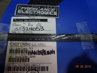
74AHCT244N
Part #
74AHCT244N
Description
Category
IC
Availability
In Stock
Qty
5
Qty
Price
1 +
$1.60721
Manufacturer
Available
Qty
ZX
Date Code: 8502
Freelance Stock:
5
Ships Immediately
Add to Cart
Related Items
Philips Semiconductor
IC
74AHC126PW-T
$0.84953
Philips Semiconductor
IC
74AHCT1G04GW
$1.30456
Military Spec
IC
74AHCT240N
$1.60721
Philips Semiconductor
IC
74AHCT245D
$0.18495
NXP SEMICONDUCTORS
IC
74AHCT541D
$0.27129
NXP SEMICONDUCTORS
IC
74AHCT541PW
$0.98121